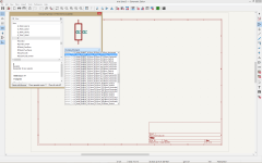
I am trying to update PCB from schematic but I am receiving errors that footprint libraries are not found. The errors are the following:
The following is the version information:
Code:
Info: Processing component “R3:/627FF10F:Resistors_THT:R_Axial_DIN0414_L11.9mm_D4.5mm_P15.24mm_Horizontal”.
Add C1 (footprint “Capacitors_THT:CP_Axial_L18.0mm_D8.0mm_P25.00mm_Horizontal”).
Add R1 (footprint “Resistors_THT:R_Axial_DIN0414_L11.9mm_D4.5mm_P15.24mm_Horizontal”).
Add R2 (footprint “Resistors_THT:R_Axial_DIN0414_L11.9mm_D4.5mm_P15.24mm_Horizontal”).
Add R3 (footprint “Resistors_THT:R_Axial_DIN0414_L11.9mm_D4.5mm_P15.24mm_Horizontal”).
Error: Cannot add Q1 (footprint “Package_TO_SOT_THT:TO-92_Inline” not found).

Total warnings: 0, errors: 1.
Error: Errors occurred during the netlist update. Unless you fix them your board will not be consistent with the schematics.
The following is the version information:
Code:
Application: KiCad
Version: 5.1.9+dfsg1-1, release build
Libraries:
    wxWidgets 3.0.5
    libcurl/7.74.0 OpenSSL/1.1.1n zlib/1.2.11 brotli/1.0.9 libidn2/2.3.0 libpsl/0.21.0 (+libidn2/2.3.0) libssh2/1.9.0 nghttp2/1.43.0 librtmp/2.3
Platform: Linux 5.10.0-14-amd64 x86_64, 64 bit, Little endian, wxGTK
Build Info:
    wxWidgets: 3.0.5 (wchar_t,wx containers,compatible with 2.8) GTK+ 3.24
    Boost: 1.74.0
    OpenCASCADE Technology: 7.5.0
    Curl: 7.72.0
    Compiler: GCC 10.2.1 with C++ ABI 1014
Build settings:
    USE_WX_GRAPHICS_CONTEXT=OFF
    USE_WX_OVERLAY=ON
    KICAD_SCRIPTING=ON
    KICAD_SCRIPTING_MODULES=ON
    KICAD_SCRIPTING_PYTHON3=ON
    KICAD_SCRIPTING_WXPYTHON=ON
    KICAD_SCRIPTING_WXPYTHON_PHOENIX=ON
    KICAD_SCRIPTING_ACTION_MENU=ON
    BUILD_GITHUB_PLUGIN=ON
    KICAD_USE_OCE=OFF
    KICAD_USE_OCC=ON
KICAD_SPICE=ONI clicked preferences > Manage Footprint Libraries but I still do not know what I should do. Checking online for the page represented by ${KIGITHUB}, I found, it does not list any footprints, implying the URL for ${KIGITHUB} is incorrect. This is my inexpert conclusion, but as all the rest of the 7 billion human beings, I can be wrong.
Added Later:
My impression is KiCad reads these libraries online from the internet. The URL has been changed to gitlab instead of github. I am searching for an archive containing these libraries so that I would be able to save them on my local computer and avoid having to depend on an internet connection. However, I did not find any archives, but only individual files.
Last edited:
Did you upgrade from Version 4 to Version 5 or was it a clean install ? There appears to be some changes to the library configurations.
Some info for Linux users - I installed KiCad 5 but there are no libraries. (The default option for sym lib table setup is disabled)
Some info for Linux users - I installed KiCad 5 but there are no libraries. (The default option for sym lib table setup is disabled)
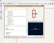
Place ==> Add symbol ==> then click on "no default footprint" and make a choiceI am trying to update PCB from schematic but I am receiving errors that footprint libraries are not found. The errors are the following:
Attachments
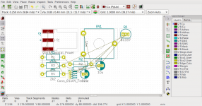
The hurdle of unfound footprints has been overcome and now I have PCB New showing a bunch of components with straight lines joining them. However, this is far from a ready designed PCB! What am I supposed to do with these components, and is there a way to tell PC New to automatically create a PCB, so that, I would only need to edit where necessary?
Added Later:
Very slowly, I am learning. The next thing to learn is how to define the physical edges of a PCB. There is no rectange tool in my installation or I have not been able to find it.
Added Later:
Very slowly, I am learning. The next thing to learn is how to define the physical edges of a PCB. There is no rectange tool in my installation or I have not been able to find it.
Last edited:
Now comes the fun part, I guess you just have bunch of components on a black background with white lines connecting them all together.
First you'll need to define the physical pcb outline otherwise the board will have infinite dimensions. On the right side you'll see a bunch of layers, find the one labelled "Edge Cuts" make sure it's ticked then "select" this layer (indicated by blue arrow) and then select the icon with the "4 dots and purple lines" (add graphic lines) and then draw the shape of your pcb board. To make it easier to connect the lines together use a 1mm grid setting.
First you'll need to define the physical pcb outline otherwise the board will have infinite dimensions. On the right side you'll see a bunch of layers, find the one labelled "Edge Cuts" make sure it's ticked then "select" this layer (indicated by blue arrow) and then select the icon with the "4 dots and purple lines" (add graphic lines) and then draw the shape of your pcb board. To make it easier to connect the lines together use a 1mm grid setting.
Okay, Just click on a component and it should be highlighted, now you can move the component anywhere on the pcb by holding the mouse button down, be mindful that you can also select just a pad of a component if you need to see the properties.
You can also click a component, then right click your mouse and this will bring up another menu, for example to rotate the component.
At this point you may want to define the board setup (Design Rules), so you can have multiple predefined pcb track sizes, via sizes and clearances. Otherwise you'll have limited options at this stage. These design rules are not global and are set on every specific pcb project.
In PCBnew goto > File > Board Setup
Last edited:
I am on Devuan (Linux). Upgrading to a newer version is not straightforward and may require incompatible executable function libraries (in Windows known as DLLs). Upgrading may require me to download the source archives and to try to compile them against the local libraries. However, again, this is not easy, and is often the work of dedicated developers known as package maintainers.Version 6.0.4 is more user friendly.
Added Later:
I have all tracks showing as simple very thin straight lines. How can these lines be made to look like real PCB tracks?
Last edited:
I have no idea about windows, I am Mac. KiCad supply many OS friendly systems, have a look and they even write different editions for oddball OS's; https://www.kicad.org/download/
Edit their width ( right click). I think you might read Help file or tutorial first, because you will have tens of similar questions before making your first PCB. Try to do the job yourself, help file is powerful.I have all tracks showing as simple very thin straight lines. How can these lines be made to look like real PCB tracks?
Sounds like they are still the rats nest lines, not traces.I have all tracks showing as simple very thin straight lines. How can these lines be made to look like real PCB tracks?
See if you can find a step by step example in the tutorial to work through.
There are many, many steps and choices to be made in laying out a pcb.
I am studying the tutorial. Afterwards, like a student, I am going to do some PCBs in ascending order of difficulty as an exercise. Suggestions of simple schematics which can be used for these exercises will help me a lot.
The real projects can wait until I achieve a satisfactory level of proficiency.
The real projects can wait until I achieve a satisfactory level of proficiency.
Those thin white lines connecting pads and components are as mentioned above "ratsnest lines" or in plain English showing connections as in from>to , of course a VERY important help.
They are not tracks yet, so no width, even no layer assigned, go figure.
YOU will replace them by tracks, you choose width (I´m old style and still think in "mils", thousandths of an inch , which for decades has been the measurement standard for PCBs, not too happy at all with newfangled mm units, go figure). a common "starting" value is 40 mil , or 1 mm.
You use wider to carry higher current or lower in tight spaces, but that´s a good starting size.
So basic generic track laying procedure is conceptually straightforward, suppose you have 2 resistors, R1 and R2 in series.
You will have a thin white line going from one pin/leg/pad in R1 yo one in R2.
Now you choose a track width, a layer /typically the "solder"/bottom one" click on said pin on R1, move your mouse cursor to needed pin on R2 (both connected pins are shown by the white line) and click there.
Now you will have a track connecting R1 to R2 and that white line will disappear.
Go open a champagne bottle to celebrate, you have just laid your first track.")
Easy, huh?
TOO easy?
Well, yes and no.
For a single track, yes.
Although you still need to tidy things up.
If you literally followed the white line, chances are track was laid at any random angle; to avoid future clashes we lay it using vertical and horizontal segments as needed.
As easy as laying, say, a horizontal segment >click (it fixes that point), vertical > click and so on zigzagging until you reach destination.
Now in a real design, tracks will quickly run into each other, so you will have to "solve the maze" and search for alternate paths.
And NOW you are designing a real PCB
Start with a simple design, say a transistor single gain stage.
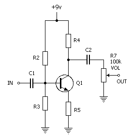
Besides basic circuit elements, you´ll need to define a ground line , input and output connectors and at least 9V battery or some kind of supply. Kicad won´t like/let you leave unterminated connections.
You will need to choose a footprint for each component, but that is not difficult, there are very popular patterns which are used over and over.
Personally I suggest resistors are either "1/4W" or "400 mil" or "10 mm", all 3 names mean basically same, transistor will be "TO92", ceramic capacitors will fit in a pattern with "200 mil pad separation", etc.
I drew and printed a ruler graduated in mils, will post an image later, which I use to quickly get real world parts size,for components I have on my workbench, faster than browsing lots of datasheets.
Do it and post first results there.
Conceptually, there´s nothing more than that, only complicated by having many components, but you´ll get there later.
Good luck.
They are not tracks yet, so no width, even no layer assigned, go figure.
YOU will replace them by tracks, you choose width (I´m old style and still think in "mils", thousandths of an inch , which for decades has been the measurement standard for PCBs, not too happy at all with newfangled mm units, go figure). a common "starting" value is 40 mil , or 1 mm.
You use wider to carry higher current or lower in tight spaces, but that´s a good starting size.
So basic generic track laying procedure is conceptually straightforward, suppose you have 2 resistors, R1 and R2 in series.
You will have a thin white line going from one pin/leg/pad in R1 yo one in R2.
Now you choose a track width, a layer /typically the "solder"/bottom one" click on said pin on R1, move your mouse cursor to needed pin on R2 (both connected pins are shown by the white line) and click there.
Now you will have a track connecting R1 to R2 and that white line will disappear.
Go open a champagne bottle to celebrate, you have just laid your first track.
Easy, huh?
TOO easy?
Well, yes and no.
For a single track, yes.
Although you still need to tidy things up.
If you literally followed the white line, chances are track was laid at any random angle; to avoid future clashes we lay it using vertical and horizontal segments as needed.
As easy as laying, say, a horizontal segment >click (it fixes that point), vertical > click and so on zigzagging until you reach destination.
Now in a real design, tracks will quickly run into each other, so you will have to "solve the maze" and search for alternate paths.
And NOW you are designing a real PCB
Start with a simple design, say a transistor single gain stage.
Besides basic circuit elements, you´ll need to define a ground line , input and output connectors and at least 9V battery or some kind of supply. Kicad won´t like/let you leave unterminated connections.
You will need to choose a footprint for each component, but that is not difficult, there are very popular patterns which are used over and over.
Personally I suggest resistors are either "1/4W" or "400 mil" or "10 mm", all 3 names mean basically same, transistor will be "TO92", ceramic capacitors will fit in a pattern with "200 mil pad separation", etc.
I drew and printed a ruler graduated in mils, will post an image later, which I use to quickly get real world parts size,for components I have on my workbench, faster than browsing lots of datasheets.
Do it and post first results there.
Conceptually, there´s nothing more than that, only complicated by having many components, but you´ll get there later.
Good luck.
Last edited:
I read the tutorial and started my first schematic as an exercise. I need to add some resistors and every time I have to open the component library to select a resistor. I would like to know if I can add similar comonents without having to every time open the component library window. Is there a shortcut? "Insert" does not work on my setup.
I beg your pardon for asking.
I beg your pardon for asking.
You can add the same component (a duplicate or copy) in the following ways:
Place mouse cursor over the component on the schematic you wish to duplicate, then right click and select "Duplicate".
or
Place mouse cursor over the component on the schematic you wish to duplicate, then press "c" on your keyboard.
This also includes all the properties of the component that is being copied.
Last edited:
The schematic posted by JMFahey has been created in Eeschema and passed the Electrical Rules Test. I am posting the resulting image of the components connected with a ratsnet. The image is what KiCad gave me. I understand the brown lines are electrical wires and the blue lines serve only as indicators for component lables, etc.
Attachments
Excellent.
Now you need to move components around, even rotating them, so you minimize connection lengths, interconnected parts are nearby, not at opposite ends of the board, and you minimize crisscrossing paths, which will ease future track layout.
Just for starters:
but in general you started fine, now practice moving things around, notice you are NOT laying tracks yet
Good layout is essential, to simplify track laying later.
EDIT: a beginner´s trick is to move parts to approximately same positions they hold in the schematic. essentiall you "redraw the schematic" but with actual parts.
Which makes things easier to see.
Not space efficient, first PCB will be larger than necessary, (who cares?) , but it will be easier, morebintuitive, to solve connectivity.
Once you solved it, you start layingb tracks, until everything is connected.
THEN you start making PCB more compact.
I remember in the old days I suffered because I tried to design the perfect PCB at once, so often run out of space between components to lay tracks , had to select blocks to separate parts, a mess.
Now I start with a table size PCB he he, which is easy peasy to solve, and then start compacting.
Now you need to move components around, even rotating them, so you minimize connection lengths, interconnected parts are nearby, not at opposite ends of the board, and you minimize crisscrossing paths, which will ease future track layout.
Just for starters:
- move Q1 from top right to bottom left, see its connection lines are too long and it has no components nearby
- just "my" preference: I try to place resistors vertical "so they look like on the schematic"
- think of future mounting , this particular example is a small Guitar signal booster, powered by 9V, mounted inside a small Hammond "pedal case", think where you want the pot , input and output jacks, they will typically be at PCB edges so they bolt to a panel.
but in general you started fine, now practice moving things around, notice you are NOT laying tracks yet
Good layout is essential, to simplify track laying later.
EDIT: a beginner´s trick is to move parts to approximately same positions they hold in the schematic. essentiall you "redraw the schematic" but with actual parts.
Which makes things easier to see.
Not space efficient, first PCB will be larger than necessary, (who cares?) , but it will be easier, morebintuitive, to solve connectivity.
Once you solved it, you start layingb tracks, until everything is connected.
THEN you start making PCB more compact.
I remember in the old days I suffered because I tried to design the perfect PCB at once, so often run out of space between components to lay tracks , had to select blocks to separate parts, a mess.
Now I start with a table size PCB he he, which is easy peasy to solve, and then start compacting.
Last edited:
- Home
- Design & Build
- Software Tools
- Using KiCad.