What about short circuit protection, is that built in or an option?
The short circuit protection is implemented in my PS regulator. More about it in my ThermalTrak amp thread.
HI Guys,
If you make PCB for 120W version could it be in same format as in post#82 with maximum PCB high 68-70mm? (2 pair outputstage)
If you make PCB for 120W version could it be in same format as in post#82 with maximum PCB high 68-70mm? (2 pair outputstage)
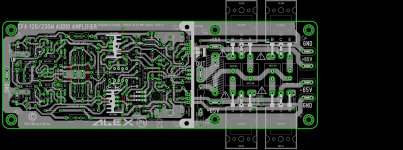
OK no problem ,could be like this ? 😉
Regards ,Alex
Yes Alex, very nice🙂
Is it possible to buy a pair of these PCB´s?
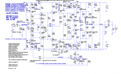
Components on the PCB disagree with parts in the diagram.
Look Q31 and R78.Check it with a scheme
Sorry for my ENG
Look Q31 and R78.Check it with a scheme
Sorry for my ENG
Components on the PCB disagree with parts in the diagram.
Look Q31 and R78.Check it with a scheme
Sorry for my ENG
Thanks🙂
Then it may not be a problem when it's only a few components🙂
Hi Guys, do you have any news for this great thread?
Did any of you build an amplifier from here yet?
Did any of you build an amplifier from here yet?
I am in the process to assemble two types of CFA, 120W latmosfet amp and 200W vmosfet amp.
I ordered the PCBs and components, and I hope in near future those amps will sing with no stability problems. Both amps use a compensation a bit different from other amps (as much as I know), combination of OIC(Output Inclusive Compensation) and MC(Miller compensation) with a twist as OIC use two pole compensation.
This Unique amp is with quite similar ISP as with other OPS variations. I did not want to go for separate IPS and OPS board as in my opinion that is not possible to do without some compromises I don't want to make.
Here is 120W TT CFA, amp with sensational low THD and very good PM and GM, in simulation, and when I finished a test with first two amp I will make the layout for this amp, in my opinion, with output power good for most DIYers.
Damir
Attachments
Very impressive design - as allways with you dadod🙂
It´s interesting the way you use advanced "compensation" are these helping for your low distortion figures?
You don´t use any load resistors this time from VAS collector to ground to minimize loop gain?
Can you also show curves with open loop bandwith and open loop gain?
Thanks Again
It´s interesting the way you use advanced "compensation" are these helping for your low distortion figures?
You don´t use any load resistors this time from VAS collector to ground to minimize loop gain?
Can you also show curves with open loop bandwith and open loop gain?
Thanks Again
Very impressive design - as allways with you dadod🙂
It´s interesting the way you use advanced "compensation" are these helping for your low distortion figures?
You don´t use any load resistors this time from VAS collector to ground to minimize loop gain?
Can you also show curves with open loop bandwith and open loop gain?
Thanks Again
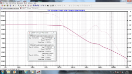
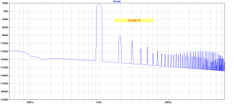
I tried partial shunt VAS compensation(look previous schematic), but with this Miller compensation(C14 R60) distortion is lower at high frequencies, and why to waste useful gain if it could be use as local NFB. 🙂
Here is the Loop Gain, I think it is more useful than the Opel Loop Gain as it shows the Phase Margin and the Gain Margin.
Damir
Attachments
Thanks dadod🙂
Please see PM from me I have sent you a schematic from NAD M3 service manual showing CF amplifier inputstage with special modifications, have you seen these before?
"notice the Circuit around Q308 I marked with yellow"
Maybe it´s something you could test in simulation program??
Please see PM from me I have sent you a schematic from NAD M3 service manual showing CF amplifier inputstage with special modifications, have you seen these before?
"notice the Circuit around Q308 I marked with yellow"
Maybe it´s something you could test in simulation program??
I tried partial shunt VAS compensation(look previous schematic), but with this Miller compensation(C14 R60) distortion is lower at high frequencies, and why to waste useful gain if it could be use as local NFB. 🙂
Here is the Loop Gain, I think it is more useful than the Opel Loop Gain as it shows the Phase Margin and the Gain Margin.
Damir
Hi Damir
The design has very good performance, congrats.
If you look closely youll notice C14 R60 shunts to ground via R43 so its not ordinary miller compensation. The only reason you have more loop gain here is the addition of the added resistance before GND. Also the loop gain plot is typical of TPC, which is nothing more than a 2 shunts. These shunts can also be called - lead lag and I have seen many other acronyms, because of the introduction of the resistance but the behaviour is typical of what is called shunt compensation. When I find the particular paper by Willy Sansen with analysis of TPC and shunt compensation Ill send you a copy.
Hi Manso,
I was thinking in that direction too and I think you are right. If I connect this Miller compensation directly to the EF bases(now with two RC circuit) I could not get the LG curve I want. The TPOIC resistor(R43) play a role in this shunt behavior. I am just finishing my later MOSFET amp with the same compensation and it will show if the concept is stable (according to D. Self it should not be).
Thank you for your offer to send me a copy
BR Damir
Upgraded version, THD below 1 ppm at 50W at all frequencies.
I can't get better than that with any amp I simulated, VFA or CFA.
I can't get better than that with any amp I simulated, VFA or CFA.
Attachments

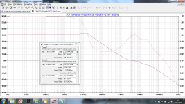
Upgraded version, THD below 1 ppm at 50W at all frequencies.
I can't get better than that with any amp I simulated, VFA or CFA.
Wow truly impressive Work🙂
Do you also make / sell PCB's for this?
Hi Manso,
I was thinking in that direction too and I think you are right. If I connect this Miller compensation directly to the EF bases(now with two RC circuit) I could not get the LG curve I want. The TPOIC resistor(R43) play a role in this shunt behavior. I am just finishing my later MOSFET amp with the same compensation and it will show if the concept is stable (according to D. Self it should not be).
Thank you for your offer to send me a copy
BR Damir
I just forgot to mention, the compensation concept is sound. It is working and it is stable in VMOSFET CFA 200W amp and it should work here.
- Home
- Amplifiers
- Solid State
- Unique CFA 120/230W amp