Hi ronovar,
I appreciate the feedback. Always something new to learn.
I like the simplicity of this design. But have been tinkering in sims with variations on it. Cascoding of the JFETs is one of them, as you suggested. The main benefit here (from my perspective) is to run at higher voltages for more output. I was envisioning a 2 pair design with the OPS running at 49V to 56V.
Regarding the VAS Cascode, I attached a pic of my quick sim. I image Q5 and Q6 could be replaced with TO-92 devices and R14 could be a current regulating diode. I also did not do a loop gain analysis. Not sure if C3 and C4 would need adjusting.
Question for the experts - since my version uses boosted IPS-VAS rails, would the cascode benefit for a higher reference voltage? I could always increase the V2 boost to allow for a higher voltage without sacrificing output potential.
Attachments

@brian92fs
ECX10N20/ECX10P20 has built in protection diodes.
So there is no need for any other zener diodes to protect.
Read here Features: https://gb.profusion.uk/uk/ecx10n20
ECX10N20/ECX10P20 has built in protection diodes.
So there is no need for any other zener diodes to protect.
Read here Features: https://gb.profusion.uk/uk/ecx10n20
Last edited:
Hi lineup- yep I figured that out after the PCBs were delivered. I have it in my notes for changes if I have another batch made.
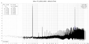
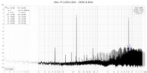
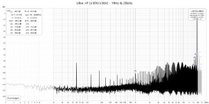
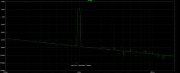
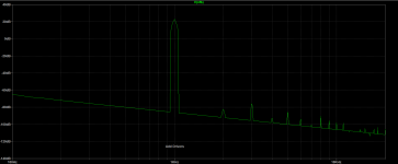
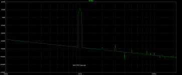
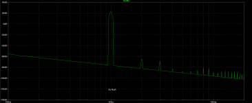
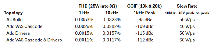
So, I thought it would be interesting to do a deeper dive into comparing topologies in simulations. All of these are running with 30V main rails, 36V IPS-VAS-Driver rails, and 500mA of bias. The compensation was adjusted for 67 degrees and 15dB to 20dB of margin. I compared these variants:
Of all of these, #3 seems to be the smallest change with the biggest impact. It retains the as-built distortion spectrum, but lowers the overall THD and improves IMD distortion by 20dB.
#4 improves it further with most reduction THD, though the change seems to be all even order harmonics reduction. It also has the best slew rate.
I believe #3 and #4 also provide less dependence on matched gain in the VAS devices.
However, the as-built isn't bad either 🙂.
- As Built
- Add VAS Cascode
- Add Drivers
- Add VAS Cascode and Drivers
Of all of these, #3 seems to be the smallest change with the biggest impact. It retains the as-built distortion spectrum, but lowers the overall THD and improves IMD distortion by 20dB.
#4 improves it further with most reduction THD, though the change seems to be all even order harmonics reduction. It also has the best slew rate.
I believe #3 and #4 also provide less dependence on matched gain in the VAS devices.
However, the as-built isn't bad either 🙂.
Attachments
Last edited:
If anyone is interested in this amplifier we can soon offer a build guide.
Just wait for some time.
Brian is working on it 🙂
There might even be a new thread to build the Ultra amp.
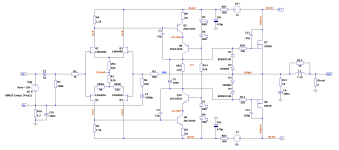
Here is my last schematic:
Just wait for some time.
Brian is working on it 🙂
There might even be a new thread to build the Ultra amp.
Here is my last schematic:
Attachments

Last edited:
Guide and BOM is nearly done. One note, the PCB's I've produced are very similar to Lineups schematic posted above, but do have some tweaks. This was done mostly for real world considerations and results of testing. For example, to add protective elements, improve thermal & DC stability and address the availability of parts.
I have started working in a layout for a simple version (same rail voltage for driver and power section). First attempt doesn't look too bad.
Size is 50mmx165mm.
Would appreciate a 2nd pair of eyes on the schematic. If the schematic is correct, KiCAD's rule checker will ensure the PCB is not wrong as well.
EDIT: Found an error: lower Zener and 1N4004 have wrong direction.
Thanks to @lineup for the schematic and @brian92fs for additional tweaks.
Last edited:
Lower noise. That was the main reason.
I also seem to remember improvements elsewhere... I thought it was THD. Might have been THD at higher frequency or higher power levels. I can't recall.
I'll add that some designers won't see noise as an issue with power amps. My thinking was that it some do see this as a benefit and it only takes a slightly more expense resistor.
I had just noticed, I asked in the wrong thread and moved the post to your build thread. Sorry for potentially confusing readers here. The question Brian has answered above is
"why did you change the NFB resistors from lineup's 12k/1k to so much lower values like 500R/100R? I do not mean ratio, but magnitude.
If I use the original values, the THD very slightly falls in the sim (which I do not care about), but they would not need to be 1W or 2W."
"why did you change the NFB resistors from lineup's 12k/1k to so much lower values like 500R/100R? I do not mean ratio, but magnitude.
If I use the original values, the THD very slightly falls in the sim (which I do not care about), but they would not need to be 1W or 2W."
I took a look and the other tradeoff is gain margin. It erodes a bit as the relative values of the feedback resistors increase. For example, if you increase to 10k/2k, you'd need to increase the compensation caps from 15p to 18p to maintain the same loop gain margins.
Overall, the impact is small which ever direction you choose. It's not critical.
Overall, the impact is small which ever direction you choose. It's not critical.
Pondering this further, using larger resistor values does have the benefit of a smaller (and probably cheaper) feedback cap. I'll have to think on this and run a few more sims to make sure there wasn't some other reason I choose this lower value.
It could very well be an idea I had that I neglected to revisit once the dust settled.
It could very well be an idea I had that I neglected to revisit once the dust settled.
For me in Spice it looks like higher values work just a bit better, not worse. The FFT has a similar noise floor (or where else would I see the noise you referred to?) and THD is slightly lower.
Another thing I noticed is that with slighly lower VAS current (like 18mA), THD is also slightly lower.
EDIT: The current waveform gets more distorted towards lower values. Not sure if that is a Spice issue? Or is there a clear reason why the current needs to be above 24mA?
Another thing I noticed is that with slighly lower VAS current (like 18mA), THD is also slightly lower.
EDIT: The current waveform gets more distorted towards lower values. Not sure if that is a Spice issue? Or is there a clear reason why the current needs to be above 24mA?
Last edited:
What is the purpose of D1, 2, 9, 10 and why D3,4,5,6 the protection diodes are built into the MOSFETS die, see data sheet. D7 and D8 should be omitted they are in parallel with the MOSFET body diode.
C9 and C10 just adds to more gate source capacitance making it even harder to turn off. That is why the VAS needs 18mA, Rule of thumb is that VAS is rater 10mA, R11 should be 270R while R12 should be 330 R due to the bottom MMOSFET having lower gate capacitance. This is not from siming it, it is real life. Also R7 and 8 should be much higher so that C5 can be made smaller with better stability.
Diodes across capacitors was one of Randy Sloans odd design ideas but could never tell me the reason for them just to protect the capacitor from what - nothing. A better implementation is two capacitors back to back making them non-polar.
I am guessing RT8 and R19 at 100R would decrease THD and bring the VAS down to about 10mA the optimum value. Yjr reason for your lower resistance is to discharge the additional caps pasted around the MOSFET,
Why C3 and C4 it duplicates C12 and C13
That was my two cents worth, otherwise a nice design
Last edited:
Diodes across cap (D1/2) makes sense to me when the cap is high value and a low voltage cap is used to keep is physically smaller. If there is a fault condition with high DC on the output, it saves the cap from failing. Now if R7/8 are increased and a smaller cap is used that can be rated for the main rail voltages, then I agree these are unnecessary.
The MOSFET gate-source and drain-source caps are unnecessary if Exicon outputs are used. Not sure if this is the case with other out of production devices - assuming a builder was using NOS parts.
D9/10 protect the rails if there is a fault on one rail. Bob Cordell suggests their use. Just protection - not needed for the amp to function normally. Many designs do not use these.
For the lateral MOSFET gate stoppers, there isn't a clear consensus among designers on exact values. I've seen anything from 100R to 470R in these positions. I suggest 330/220 for TO-247 devices and you are suggesting 330/270. I don't think either is wrong. Just try to keep the N channel stopper bigger than the P channel to account for differences in capacitance as you pointed out.
I know we disagree on C9/10. I see them as being cautious and not really causing much harm. But I can't say for certain they are necessary.
For VAS currents, I don't think the exact value is critical. I choose to use around 25mA. But running a bit lower shouldn't make a significant difference. We are assuming that sims reflect real-life. Ideally, we'd test this on the bench if we really wanted to dial in peak performance.
As this is not a ultra-low distortion design, I didn't feel this was necessary and found around 25mA to be suitable. But that's just my opinion - no magic here. I'm guessing performance won't be materially different if 18mA is used.
As this is not a ultra-low distortion design, I didn't feel this was necessary and found around 25mA to be suitable. But that's just my opinion - no magic here. I'm guessing performance won't be materially different if 18mA is used.
BTW - thank you @mz543578854 for digging into this. I don't claim to have gotten everything right. I'm sure there are improvements that can be made.
- Home
- Amplifiers
- Solid State
- Ultra Amplifier with JFET input and Lateral MOSFET out