thank you for reply Andrew
original UGS using 22 R as source to P channel j109 as Is In first post
If we choose j74 with Idss of 10.5 and k170 with Idss of 9.8 we need R degen of 2.3 R added to 22R which gives total 24.3 R
yes , at least how I'm understanding that
or , you can just use matched Idss ones , without Rs correction , as in Papa's UGS
there is enough feedback to correct things ........ and who'll be judge what's better - absolute symmetry , or less perfect one
you are overlooking the source degeneration of 47r fitted to the Nchannel devicesyes , at least how I'm understanding that
one does not normally use NFB to hide a poor performance inside the amplifier. One strives to create a good performance and then applies NFB to set the gain and output impedance and any attenuation of distortions is just given for free. Especially in a low feedback design as are many of Pass' amplifiers.or , you can just use matched Idss ones , without Rs correction , as in Papa's UGS
there is enough feedback to correct things ........ and who'll be judge what's better - absolute symmetry , or less perfect one
Im looking for the latest software to use with the crystalfontz display.
If anyone still have it I would really appreciate a copy. Or maybe point to where I can download it.
One more.. Did anyone use a "usb to 36 pin connector" to program the atmel?
Best Regards
David
If anyone still have it I would really appreciate a copy. Or maybe point to where I can download it.
One more.. Did anyone use a "usb to 36 pin connector" to program the atmel?
Best Regards
David
Last edited:
I have built a version of this using using BC550/560 instead of the ZTX parts with slightly more than 2x current gain to allow 10mA through the output transistors. The current mirror transistors are thermally bonded (although perhaps not perfectly) and matched for Vbe, but I still ended up with thermal runaway. Is there anything else I should look for to eliminate this issue?
EDIT: Forgot to say that rails are lower at around +/-18V, so I adjusted the values of RD and RE (referring to the original schematic on page 1) to give around 13V on the JFET drains and about 2.5x current gain.
EDIT: Forgot to say that rails are lower at around +/-18V, so I adjusted the values of RD and RE (referring to the original schematic on page 1) to give around 13V on the JFET drains and about 2.5x current gain.
Last edited:
CMRR
Hi.
I am doing some testing on a UGS gain stage for a friend and we are trying to get the CMRR as good as possible. By adjusting the R_FB on either side the gain can be balanced and I was able to get the CMRR down to -76dB by inserting a 100k potentiometer in place of one of the resistances yesterday. I am now considering if I should to put a 2M potentiometer in parallell with one of the R_FB or if I should put a 500 ohm potentiometer in series with one.
Anyone?
UGS THD+N curve
I have measured the THD+N on the UGS gain buffer.
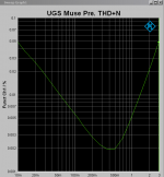
This measurement is done with a high quality R&S UPV audio analyzer.
We can see that the noise level is very good, but distortion starts to rise above 600mV and ends up at about 0,02% at 2V RMS.
This is certainly acceptable, it would be nice if there is a way to keep distortion lower up to about 2V.
Does someone have some advice they could share?
Regarding my question about CMRR above I ended up inserting the potentiometer in series. It works fine and makes it easy to adjust for optimum CMRR.
I have measured the THD+N on the UGS gain buffer.

This measurement is done with a high quality R&S UPV audio analyzer.
We can see that the noise level is very good, but distortion starts to rise above 600mV and ends up at about 0,02% at 2V RMS.
This is certainly acceptable, it would be nice if there is a way to keep distortion lower up to about 2V.
Does someone have some advice they could share?
Regarding my question about CMRR above I ended up inserting the potentiometer in series. It works fine and makes it easy to adjust for optimum CMRR.
Just a remark. This UGS version is run at +-24V supply. Usually Pass Labs runs them at +-32V. Maybe the supply has an impact to where the sweet spot is localized. If you look at the original XP30 THD (from Stereophile reviews) you'll see that the minimum THD is higher in voltage, around 5V...
Also I don't know if your measurement was done SE or BAL. Balanced should be better because of the X architecture that should cancel distortion even more.
Finally I don't know if this preamp was modified to replace the output resistors from 1K to 100K. Alex realized it was an error to have these resistors at 1K (R29-R32). They load the UGS too much...
Attachments
Last edited:
Thank you for your remark. The measurement was done balanced.
I can try to take the USG module out of the preamplifier and measure it alone with higher supply voltage and see what happens.
I am busy with another project a couple of days now, but I will do more measurements soon.
I can try to take the USG module out of the preamplifier and measure it alone with higher supply voltage and see what happens.
I am busy with another project a couple of days now, but I will do more measurements soon.
Hi Guys,
I have asked before but maybe now there is news:
Does anyone know if any Wifi app has been developed for the Wifi Module ?~
I am talking about Muse version naturaly.
😕
I have asked before but maybe now there is news:
Does anyone know if any Wifi app has been developed for the Wifi Module ?~
I am talking about Muse version naturaly.
😕
I have measured the THD+N on the UGS gain buffer.
View attachment 622281
This measurement is done with a high quality R&S UPV audio analyzer.
We can see that the noise level is very good, but distortion starts to rise above 600mV and ends up at about 0,02% at 2V RMS.
This is certainly acceptable, it would be nice if there is a way to keep distortion lower up to about 2V.
Does someone have some advice they could share?
Regarding my question about CMRR above I ended up inserting the potentiometer in series. It works fine and makes it easy to adjust for optimum CMRR.
1V or so common value to get most amps at clipping
If you need lower distortion at higher output voltage, consider the jfets are cascoded in the Muse. So, their running voltage is lower ... Increase supply voltage to get more undistorded voltage swing.
If you drive into low impedance or long capacitive lines, consider running more bias into the jfets (if possible and safe)
Best
1V pK/pK or 1V RMS ? The Pass Labs XA160.5 is rated at 1.79V (26dB gain) for full power. I think that papa once mentioned that he always rates his amps at RMS ? Is this correct ?
Thanks for the input regarding the Muse 🙂
Regards
Johnny
UGS gain module and buffer module measured
I have taken out the gain module and measured it standalone with a variable power supply. Balanced.
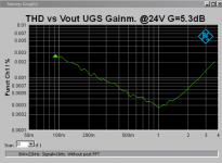
This is a THD curve with 24V rails.
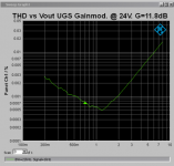
Increasing the rails to 28V did not help at all.
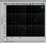
We can see that the distortion is all 3rd harmonic.
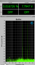
With these results it is not wise to use this module with this gain at the input. Imagine what would happen if you connect a balanced source with 4.6V RMS output like the Electrocompaniet DAC. The gain stage would bring the voltage up to 18V RMS and add massive distortion before entering the volume control chip that would have to take the voltage back down to normal levels.
I have reduced the feedback resistor to 30k for a gain of 5.3dB (1.84x), and the result is better.
Buffer
The buffer module is much better.
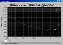
This is a THD+N as opposed to the THD measurements above. We can see a slight increase between 3 and 5 volts but otherwise this module matches the internal noise in my R&S UPV measurement equipment. (It is equipped with the "low distortion" generator)
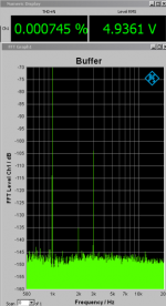
At 5V we can see that it is the 3rd harmonic that start to rise.
I can't help to think that it would be better to use the buffer module on the input before the volume chip and use the gain module after the volume chip.
In that case we would get the best from both modules. Low distortion from the buffer on the input up to the voltage swing we have from balanced sources (up to 5V). The volume chip will lower the voltage to whatever desired voltage and then the gain module will work in its more comfortable 0 to 3V range. Most power amplifiers do not need more that 2V to bring the output to clipping.
Thoughts?
I have taken out the gain module and measured it standalone with a variable power supply. Balanced.
This is a THD curve with 24V rails.

Increasing the rails to 28V did not help at all.

We can see that the distortion is all 3rd harmonic.

With these results it is not wise to use this module with this gain at the input. Imagine what would happen if you connect a balanced source with 4.6V RMS output like the Electrocompaniet DAC. The gain stage would bring the voltage up to 18V RMS and add massive distortion before entering the volume control chip that would have to take the voltage back down to normal levels.
I have reduced the feedback resistor to 30k for a gain of 5.3dB (1.84x), and the result is better.

Buffer
The buffer module is much better.

This is a THD+N as opposed to the THD measurements above. We can see a slight increase between 3 and 5 volts but otherwise this module matches the internal noise in my R&S UPV measurement equipment. (It is equipped with the "low distortion" generator)
At 5V we can see that it is the 3rd harmonic that start to rise.

I can't help to think that it would be better to use the buffer module on the input before the volume chip and use the gain module after the volume chip.
In that case we would get the best from both modules. Low distortion from the buffer on the input up to the voltage swing we have from balanced sources (up to 5V). The volume chip will lower the voltage to whatever desired voltage and then the gain module will work in its more comfortable 0 to 3V range. Most power amplifiers do not need more that 2V to bring the output to clipping.
Thoughts?
I have taken out the gain module and measured it standalone with a variable power supply. Balanced.
This is a THD curve with 24V rails.
View attachment 623810
Increasing the rails to 28V did not help at all.
View attachment 623811
We can see that the distortion is all 3rd harmonic.
View attachment 623812
With these results it is not wise to use this module with this gain at the input. Imagine what would happen if you connect a balanced source with 4.6V RMS output like the Electrocompaniet DAC. The gain stage would bring the voltage up to 18V RMS and add massive distortion before entering the volume control chip that would have to take the voltage back down to normal levels.
I have reduced the feedback resistor to 30k for a gain of 5.3dB (1.84x), and the result is better.
View attachment 623815
Buffer
The buffer module is much better.
View attachment 623816
This is a THD+N as opposed to the THD measurements above. We can see a slight increase between 3 and 5 volts but otherwise this module matches the internal noise in my R&S UPV measurement equipment. (It is equipped with the "low distortion" generator)
At 5V we can see that it is the 3rd harmonic that start to rise.
View attachment 623818
I can't help to think that it would be better to use the buffer module on the input before the volume chip and use the gain module after the volume chip.
In that case we would get the best from both modules. Low distortion from the buffer on the input up to the voltage swing we have from balanced sources (up to 5V). The volume chip will lower the voltage to whatever desired voltage and then the gain module will work in its more comfortable 0 to 3V range. Most power amplifiers do not need more that 2V to bring the output to clipping.
Thoughts?
Ideally,
Buffer in -> volume control --> UGS gain ---> Buffer out
The balanced topology leaves out 3rd harmonic résidus at the output, by design
And almost nulls out 2nd
Ideally,
Buffer in -> volume control --> UGS gain ---> Buffer out
The balanced topology leaves out 3rd harmonic résidus at the output, by design
And almost nulls out 2nd
Buffer in -> volume control --> UGS gain ---> Buffer out
That is three stages.
What about only one stage.
Source -> volume control -> UGS gain -> Output.
I am not convinced the buffer on the input is needed. The volume controller chip represents a linear 20k resistive load and I don't see that this can cause problems for any source.
My thoughts is that the output buffer is not needed either. We don't have long cables and the power amp input resistance is 20k.
I measured the UGS gain module into 600 ohm load and while it certainly had a little problem with that it was still acceptable.
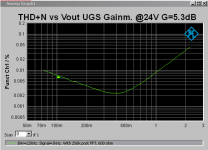
With this result into 600 ohm it should be perfectly capable of driving 20k.
The balanced topology leaves out 3rd harmonic résidus at the output, by design. And almost nulls out 2nd
We can see that the 2nd harmonic distortion from the gain module is nulled out, but we have a lot of 3rd harmonic. How can this be then? Both modules in the amp are like this.
- Home
- Amplifiers
- Pass Labs
- UGS adventures
