I used your FQA schematic with the polarity reverse on the PSU.
Edit: your test jig schematic at a lower 2.1mA.
Edit/edit - I meant your J113 matching schematic. I’m a little confused as you can see.
Edit: your test jig schematic at a lower 2.1mA.
Edit/edit - I meant your J113 matching schematic. I’m a little confused as you can see.
Last edited:
In the GB thread, I already mentioned that you should match Idss and Vp of the GR grade 2SK109.
Interest for potential GB for UDNess PCBs and matched FETs.
How ? See Fig. 5 of the Borbely article :
JFETs: The New Frontier, Part 1 | audioXpress
Patrick
Interest for potential GB for UDNess PCBs and matched FETs.
How ? See Fig. 5 of the Borbely article :
JFETs: The New Frontier, Part 1 | audioXpress
Patrick
A mosfet matching circuit is no use for JFETs.
Read the Borbely article above.
Patrick
Ok - I will re-read, thanks for posting for me. I was going by your write-up, saying to match at Vgs at 2mA.
I misspoke above - I used your J113 matching schematic, using clips to the SMD testing jig.
I need to read though your links again, and get a better understanding it appears - Thanks again.
Read the Borbely articles first.
Everyone building amps with JFETs should read both Part 1 and Part 2, if they haven't already.
😉
Patrick
Everyone building amps with JFETs should read both Part 1 and Part 2, if they haven't already.
😉
Patrick
Will do - I am constantly learning and that is why I wanted to “match” my own on this project, knowing it would force me to learn something new. In reality-it is making me learn a lot of new things.
😉
This is, for me at least, the right attitude to DIY.
And this is the kind of DIY that I want to support, even if it costs me more time than otherwise.
Patrick
This is, for me at least, the right attitude to DIY.
And this is the kind of DIY that I want to support, even if it costs me more time than otherwise.
Patrick
In the GB thread, I already mentioned that you should match Idss and Vp of the GR grade 2SK109.
Interest for potential GB for UDNess PCBs and matched FETs.
How ? See Fig. 5 of the Borbely article :
JFETs: The New Frontier, Part 1 | audioXpress
Patrick
Re-reading through the whole thread and not sure how I missed this, but I bought "Y" grade instead of "GR" grade 2SK209s. Did I just mess up the whole thing and need to re-order, or does this just limit my possible matches? I bought 50, knowing I would mess up some - just thought it would be due to magic smoke, not missing a correct part in my order.
I have read through the thread again and the build guide and the only reference other than "match" I can find is "match Vgs at 2mA" next to them in the BOM listing.
Is there a minimum/maximum Idss, or can I match 4 within +/-5% and be safe?
Now that my mosfet testing setup is working - I need to test the J113s to make sure I use >8.5mA Idss per the group buy thread.
Anyone want to weigh in on the “Y” vs. “GR” grade question?
My “Y” grade Idss measured from 1.61-2.71mA. With most close matches in the 1.75-1.85mA range. Can I use these?
I just checked Mouser and the “GR” grade is out of stock until Aug-17th.
My J113s measured Idss from 9.3-17.7mA - so all 20 look useable.
My FQAs matching gave me 4-5 very close matched pairs and a couple pair of good matches out of 20 ordered.
It is important to understand rather than just have numbers given.
Which is why Spice files were posted.
The document said that the J113 has a nominal current of 6.5mA.
When using 4x 2SK209 for Q2 + Q3, and assuming equal current sharing, each 2SK209 will get 1.6mA.
Since J113 is used to adjust DC offset, one has to allow some variations from 6.5mA.
Say 25%, which means 2mA for each 2SK209.
So yes, you can use 2SK209Y.
But I would at least pick those with min. 2mA Idss.
If you do want to use those with 1.7mA, you should increase R33 to 2k.
No idea how the distortion spectrum might change.
But probably not much.
Patrick
Thanks for walking me through this - I am reading and re-reading what you wrote (entire thread and write-up for a fourth time) and learning something new each time. So thanks for teaching as much as answering.
I continue to find a "tolerance" for matching. Some say 2%, some say 5% and Im guessing it depends on the job they are doing and the actual transistor.
So, how close would you want to match the 2SK209's? I have a matched quads real close to 2.0mA - one quad is 1.89-1.92mA and the other quad is either 1.84-1.86mA or 1.95-2.03mA? Is it better to be closer to 2.0mA and not as matched, or further from 2.0mA but a closer match to each other?
I have other close quad matches, but the closest ones are lower mA (1.6 to 1.8, but within 0.003-0.005mA) and going higher Idss they aren't as close of a quad match (2.1 up to 2.7, but off by 0.03-0.07mA).
Thinking, wiith your suggestion above -- maybe put sockets in for R33, then I could revise the resistor value as need somewhere between 1.6k and 2.0k?
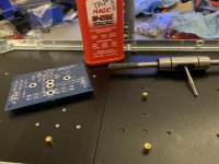
I finally got some real work done on this amp. I have spent a month learning how to match, buying all the parts for a constant current and learning to read a schematic and bread board the circuit.
First time to solder smd components, nerve wracking but I get continuity on all the solder tabs, so it should be good.
I ended up matching the 2sk209s at 1.82and 1.85mA, because they were the closest quads matching together and to the 2mA goal. We will see if I need to adjust R33 up a little.
I have verified every component prior to putting them in and matching them across the two boards to try and get them as close to matching as possible.
Still have a lot of work to do - just thought some pics might encourage someone else’s to start this project.
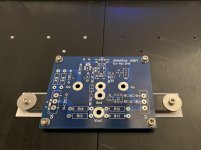
Great board design, solder very easy and plenty of room for every part.
Thanks for posting for the diy folks like me and for answering all my questions.


First time to solder smd components, nerve wracking but I get continuity on all the solder tabs, so it should be good.
I ended up matching the 2sk209s at 1.82and 1.85mA, because they were the closest quads matching together and to the 2mA goal. We will see if I need to adjust R33 up a little.
I have verified every component prior to putting them in and matching them across the two boards to try and get them as close to matching as possible.
Still have a lot of work to do - just thought some pics might encourage someone else’s to start this project.
Great board design, solder very easy and plenty of room for every part.
Thanks for posting for the diy folks like me and for answering all my questions.
Last edited:
I'm definitely keeping track. Truly appreciate you posting the progress. Learning from your hard work.

I’m also following along. I had some boards made up by JLCPCB. Thank you for the gerbers and the development and documentation on this project Patrick! Just finished tapping some extra holes for the boards in a 5U deluxe chassis from the diyA store. This was my first time tapping. It went very well. I invested in some good quality taps, used the right size drill bit for the holes, and used plenty of tapping fluid. Looking at the new holes you can’t tell them apart from the ones that came from hifi2000. 😀
The holes for the mosfets were original to the sinks and fit the required spacing perfectly.
The holes for the mosfets were original to the sinks and fit the required spacing perfectly.
Attachments
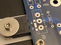
If you leave out the power MOSFETs first during soldering, you will find that it is easier to adjust and trim the front end on its own.
Especially if you have matched the power devices and know the required Vgs for bias.
You can actually set the voltage across R33 to the correct value before putting in the MOSFETs.
Patrick
Especially if you have matched the power devices and know the required Vgs for bias.
You can actually set the voltage across R33 to the correct value before putting in the MOSFETs.
Patrick
And I suggest using 8mm standoffs.
6mm is absolute minimum.
You need some gap between PCB and heat sink.
Or the space in between will actually get hot.
Patrick
6mm is absolute minimum.
You need some gap between PCB and heat sink.
Or the space in between will actually get hot.
Patrick
- Home
- Amplifiers
- Solid State
- UDNeSS, or You don't need Semisouth's