In class d, forget all about single sided, it just cannot be done.
Absolute minimum double sided is mandatory with either top or bottom layer beeing a uninterrupted ground plane, well atleast as uninterrupted as possible.
Also don't bother with home etching boards, in the end, placing an order with itead studio will end up cheaper.
Absolute minimum double sided is mandatory with either top or bottom layer beeing a uninterrupted ground plane, well atleast as uninterrupted as possible.
Also don't bother with home etching boards, in the end, placing an order with itead studio will end up cheaper.
Hi Tekko:
I can use the whole top layer for gnd pane, should I do that or do I need to divide high power & low power gnd? As described in iraudamp9.
Okay and how to solve power loop puzzle?
Would be great if you can give a ref of good class D pcb without SMD?
Thanks
Raj
I can use the whole top layer for gnd pane, should I do that or do I need to divide high power & low power gnd? As described in iraudamp9.
Okay and how to solve power loop puzzle?
Would be great if you can give a ref of good class D pcb without SMD?
Thanks
Raj
I've learned that you cannot get away from smd in order to make a good low emi class d as the leads on through hole components have significant inductance above 20kHz.
No point in dividing the ground plane, best to have it all continous and have everything GND connect to it, however try to keep the current loops as short as possible.
No point in dividing the ground plane, best to have it all continous and have everything GND connect to it, however try to keep the current loops as short as possible.
Hi Insomnia,
Thank you for using AUD600 amp
I am not discouraging you, your PCB design is not good for class D big GND loop will create more EMI in to the input and it will create cross talk when you using 2nd CH. Using Ground plane for reducing EMI
2. Use c18 close to the MOSFET for reducing EMI & RF
3. I am not suggesting crowbar for class D b'cause any issues causes in your PCB/components will create -Ve supply comes in SP line and it will damage 7414,2110 and MOSFET.
Regards
MANOJ
look attachment
ok have changed and add big Groundplane, is it ok now ?
But in your PCB File cant see Groundplane,
same in Detex Audio IRS 900 - 3000 Series,
only 1 Layer PCB and no Groundplane
Attachments
I've learned that you cannot get away from smd in order to make a good low emi class d as the leads on through hole components have significant inductance above 20kHz.
No point in dividing the ground plane, best to have it all continous and have everything GND connect to it, however try to keep the current loops as short as possible.
Hi Tekko:
I will use entire top copper layer for ground pane but may not be possible to short the power tracks. I can make it wider, will it help?
Is there any other suggestions?
Thanks
Raj
i have to disagree.In class d, forget all about single sided, it just cannot be done.
Absolute minimum double sided is mandatory with either top or bottom layer beeing a uninterrupted ground plane, well atleast as uninterrupted as possible.
Also don't bother with home etching boards, in the end, placing an order with itead studio will end up cheaper.
i've been building numerous class d amps, all in single sided that have worked and are still working for months now. even tried switching some of them at 800 khz and they work beautifully.
do bother with home etching. it's much easier, cheaper and faster to produce than ordering them to be made. and you can keep changing the layout and test them for any difference.
i'm only using through holes without any smd, single sided pcb and home etched. and they're happily driving my subwoofers. all 4 of them.
And they produce alot more EMI than a proper double sided board would.
And itead is definately cheaper with 30 dollars shipped for 10 boards, just the copperclad alone where i live cost more than 30 dollars alone, not to mention the chemicals required.
And itead is definately cheaper with 30 dollars shipped for 10 boards, just the copperclad alone where i live cost more than 30 dollars alone, not to mention the chemicals required.
for any kind of useful tips and design guides, google and download these PDF(s). they're application notes and design guides from IR and other manufacturers regarding class D.Hi Tekko:
I will use entire top copper layer for ground pane but may not be possible to short the power tracks. I can make it wider, will it help?
Is there any other suggestions?
Thanks
Raj
the most useful ones i've marked '#' (for me at least). they helped me much.
for PCB layout do read International Rectifier's Application Note AN-1135 - PCB Layout with IR Class D Audio Gate Drivers, it has graphics and clear explanation on the most crucial pcb parts, component layout and ground and power planes.
they do, but with proper care, optimized layout and proper sized traces and gap, it could be minimized.And they produce alot more EMI than a proper double sided board would.
And itead is definately cheaper with 30 dollars shipped for 10 boards, just the copperclad alone where i live cost more than 30 dollars alone, not to mention the chemicals required.
using just one large plane for ground isn't always gonna lower the EMI/RFI/THD.
locality is different for most people in this forum. it costs me USD$10 in parts to UV expose and etch a 15cm x 30cm pcb in 10 minutes. i could have the pcb up and running in less than a day.
and it'll take me ~30 days to order anything from the states and have them arrive at my doorstep. 😀
And i hate drilling hundreds of holes which is why i rather use smd for resistors, diodos and small value caps.
And i prefer ordering boards through itead as that way i get through plated holes and dont have to go through the hassle of using through plating repair rivets or using pieces of wire, it also gives the boards a more professional appearance than crusty homemade boards.
Also double sided boards also makes it easier to minimize current loops and thus reducing EMI/RFI.
Hi Exflaco
greetings do you have picture of pcb bottom of triell limiter want to try it
warm regards
andrew
greetings do you have picture of pcb bottom of triell limiter want to try it
warm regards
andrew
ok have changed and add big Groundplane, is it ok now ?
But in your PCB File cant see Groundplane,
same in Detex Audio IRS 900 - 3000 Series,
only 1 Layer PCB and no Groundplane
Hi Insomnia,
My PCB, without ground plane it produce less EMI (less-than @10mV) and RF(15-20cm distance no problem found on RADIO). and i am not used ground loop.
Regards
MANOJ
similar to my finding.Hi Insomnia,
My PCB, without ground plane it produce less EMI (less-than @10mV) and RF(15-20cm distance no problem found on RADIO). and i am not used ground loop.
Regards
MANOJ
one layout that i've made have a ground plane and voltage plane according to the IR app note to the letter and it's less stable compared to other layout. it's stable enough for low and medium power but start to go unstable in high power output.
not saying that ground plane and voltage plane aren't good, but you can never predict the result especially in class d. just adding a single, continuous, large plane and connect everything to it might not translate to something better.
the only way to know is to build it, test it and compare. or you could always go with a proven design like the AUD600.
Hi Insomnia,
My PCB, without ground plane it produce less EMI (less-than @10mV) and RF(15-20cm distance no problem found on RADIO). and i am not used ground loop.
Regards
MANOJ
Hi manojtm
ok will try grounbplane and see what happened with EMI,
how about DC @ output with AUD600 with no input signal, how much ?
2. I want use IXFN80N50Q2 Mosfet with 250khz switching frequency
for heavy load +/- 120 V DC.
QSC use in PL380 for Mosfet IXFN80N50Q2 9A Mosfet driver, I think with totem pole Driver can work in AUD600 too. What you think, does it work ?
3. Sorry have found this but Im confused , because have not study electronic design .
- - RSS dependent of rail voltage you used , you can calculate it , RSS = (Volt - V(zener) / 0,01 (set 10mA passing RSS) .
+ EX : If you used +/- 75V ; RSS = (75 - 5,6) / 0,01 = 6940 , so you should used 6,8K ohm / 2W 🙂
- RFB = 100K , OSC = 1K , it set Gain .
- OCP = (V bias x R ocp / 6800 ) / R (Source MOSFET) . Set limit of output current .
+ EX : I used 12V Bias , R ocp = 220 ohm , R (Source) = 0,02 ohm ( 5 x 0,1 ohm parallel)
(12 x 220 / 6800) / 0,02 = 19,4 Ampe 🙂
- Change R ocp is change limit output current .
- L output ~ 30 - 40 uH .
If want change in AUD 600 OC Limit, which resistor is it ?
For 85V and 100V and 2 Ohm load what resistor value is required ?
best regards
Attachments
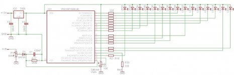
Is the Chip Microchip PIC16F1508 or PIC16F88 ?
do you share PIC file with DIY ?
can you send me
Hi Insomnia,
My PCB, without ground plane it produce less EMI (less-than @10mV) and RF(15-20cm distance no problem found on RADIO). and i am not used ground loop.
Regards
MANOJ
Hi manojtm
I can get from friend IXYS Mosfets free to test AUD600
IXFK44 N50 and IXFK48 N50
Can I use this Mosfets in AUD600 or impossibile because high Qg?
attachment IXYS Datasheet
Attachments
- Home
- Amplifiers
- Class D
- UCD 25 watts to 1200 watts using 2 mosfets