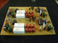
Heres my version of the board:
classdstuff :: basicclassdbrd.png picture by TheElectroNoob - Photobucket
Using regulators from the main rails, up to 35V can be used, any higher and the regulators need replacing, or removed to have an external power supply connected.
Hi Tekko,
Your pcb have good components disposed, a right way for base gerber.
Regards
Hey! Im not a pcb designer, i know i suck as pcb design.
An other reason is that the fets are below the board, but the silkscreen slaps everything on top, making it look like i put components on top of each other.
An other reason is that the fets are below the board, but the silkscreen slaps everything on top, making it look like i put components on top of each other.
Hi Tekko
Long time no see .... still doing class-d 😉
Is it the same circuit? .... I dont see the feedback line from the output (after filter) ... maybe it's on the other side.
Component layout seems better than lycankl's approach .. of course also taking
advantage of double sided pcb .... but single sided for class-d is a no go ... sorry 🙁
Hey! Im not a pcb designer, i know i suck as pcb design.
An other reason is that the fets are below the board, but the silkscreen slaps everything on top, making it look like i put components on top of each other.
Hi,
I have done sincere compliments (no irony)🙂
would be better if you take away the ground under the toroid plain.
rect to area without copper. (If I saw good blue top)
Regards
Hi,
I have done sincere compliments (no irony)🙂
would be better if you take away the ground under the toroid plain.
rect to area without copper. (If I saw good blue top)
Regards
Why take the GND layer away? .... I would have suggested to lay the coil down flat, making sure that there is a GND layer beneth, or better Vss (which is the "ground point" for much of the output driver circuit), and to make it even better place the coil on the opposite site of the other components ......
Why take the GND layer away? .... I would have suggested to lay the coil down flat, making sure that there is a GND layer beneth, or better Vss (which is the "ground point" for much of the output driver circuit), and to make it even better place the coil on the opposite site of the other components ......
Hi,
gnd flat under the toroid behaves inversely, it takes a lot of energy hf and this flows on the surface around the top plane. gnd-plane should be used with logic depending on various circumstances. (GND plane does not mean it is always good).
In this case all the other circuits on top plane, are full of HF and this increases the noise.
(Shielding function of something or against something, not in an absolute sense). eg it possible continuos top plane only if you have all components at bottom side.
Besides this there are also loops (current loop).
example, the output circuit must close with massive output (imagine that is not the same gnd)) is equal only in static DC).
ok, I certainly do not want to take a course on the development of PCB (10 years of experience at the professional level are not enough) thought it was enough to put a continuous gnd plane at the top?🙂
Last edited:
bridge mode
hi guys made the circuit and tested it 62 0 62 very power full. i still have problems with noise rf noise maybe cause i did not etch my boards . but just wondering how to bridge the scheme .because if i bridge using the hin and lin pins of the ir2110 it doesnt work good any scheme ? 🙂 steve
hi guys made the circuit and tested it 62 0 62 very power full. i still have problems with noise rf noise maybe cause i did not etch my boards . but just wondering how to bridge the scheme .because if i bridge using the hin and lin pins of the ir2110 it doesnt work good any scheme ? 🙂 steve
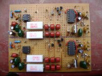
Heres a modified version of the board:
classdstuff :: basicclassdbrd1.png picture by TheElectroNoob - Photobucket
classdstuff :: basicclassdbrd1.png picture by TheElectroNoob - Photobucket
hi stewin
greetings can you post pictures of your pcb would be very helpful i am struggling
thanking you
andrew lebon
greetings can you post pictures of your pcb would be very helpful i am struggling
thanking you
andrew lebon
hi andrew try tekko's pcb desing . because mine works but i still have small issues with rf noise maybe because i did not use etched boards, the fets were mounted using the pins . but still would love to bridge the monster if there was a scheme. nice design guys steve
Heres a modified version of the board:
classdstuff :: basicclassdbrd1.png picture by TheElectroNoob - Photobucket
well,now ceck clearance on component near -vc and +vc (i see small capacitors not have right clearance at sx of pcb).
now is necessary completed first modify.(simple operation) connession at input toroide change layer with bottom and create vertical gnd with blue layer (this gnd close loop on top ) actually loop is large,(from operational up to toroidal filter). is better move 3-4mm at dx toroide.
After this, you can force both layer for output and GND output.
Last edited:
the photos
very good without pcb and very nice capacitors...I not find in Italy.. You want send me?🙂
Regards
i live in east africa i dont know how to send them but if there's a way i'll be glad to. the caps are 105 and i'm assuming they are 63vlts . but in the board they worked o.k @ 62 -0- 60 they are quite affordable here you can get 10pcs for 1$ glad to be of help stewin
Attachments
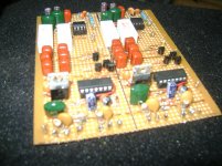
Revision 3 of my version:
classdstuff :: basicclassdbrd2.png picture by TheElectroNoob - Photobucket
This time the power for the LM311 is externally supplied.
classdstuff :: basicclassdbrd2.png picture by TheElectroNoob - Photobucket
This time the power for the LM311 is externally supplied.
hi stewin
greetings thanks for the pictures lucky you at least one project
for d class diyers affordable and once the mistakes have been rectifed it will
be a nice project how is the sound and is it really powerful bye
thanking you
andrew
greetings thanks for the pictures lucky you at least one project
for d class diyers affordable and once the mistakes have been rectifed it will
be a nice project how is the sound and is it really powerful bye
thanking you
andrew
Good work, Stewin !
Nice board! If you could get it to work then I have no doubt that the amp works well..
I design my board as a single layered and I will create myself it by ironing.. so the routing paths have to be that way.. and the spaces.. It is easy to design duel layer board but in here, there is no place to make it.. even it is, it will be very expensive so I better do it this way.. all cheep and 100% DIY.. LOL but Im thinking the best way I can rout it yet thanks to advices.
regards,
Lycanlk
- Home
- Amplifiers
- Class D
- UCD 25 watts to 1200 watts using 2 mosfets