Kartino-. It is possible to talk to you privately, as I would like to buy a complete project, just tell me the value in US Dollars.
Sorry that I do not sell any product.
I just do this for fun and help other people
And Pafi, you said the schematic has other issues. then please tell.
Dear Kartino,
As you wish. (I'm glad you don't refuse to face the problems.)
The first problem to mention is distortion. At 1 kHz, 60V peak output there is about 3 % THD.
This is partly due to the fact that you don't use integrator, but essentially caused by the very high and nonlinear delay.
1st stage is acceptable, but the second is terribly slow, and the delay time is nonlinearly dependent on the signal.
In a ClassD amp the delay determining operation freq should depend on signal in linear way, or low order polinomial way at least.
Other problems are the high offset drift, the low input impedance, the input-source dependent operation freq...
And as a bonus a chance for exploding, not just because there is no protection in it at all, but also R24 creates a possibility for control error: while C1 is less charged than C3, both Hin and Lin gets high level control signal, that can open both output FETs.
There are some other minor mistakes not worth to mention, because they are not harmful...
If I have time I will correct the mayor errors in the schematic.
Thanks for the IR2110 modell, I just started to use LTspice, I didn't have time to get or build it.
Attachments
Ok then.
UcD will need very good individual switching speed for the active parts. But non UcD can be less quality. For example D900 standard you cannot get it right with UcD topology. Max switching speed only upto less than 100kHz. But with non UcD, D900 can get 300kHz or more speed.
High switching freq is not a goal. It may be a tool to get high loop gain, but you didn't use this opportunity. In your case high switching freq only wastes more power without any benefit.
High switching freq (in a given feedback topology) also can be an indicator of fast internal circuits. Low delay is good for all correctly designed ClassD amps. Clocked designs are less sensitive, but for effective post-filter feedback low delay is also beneficial. UcD, like all phaseshift based selfoscillating amps requires low delay to keep near-rail freq high, but in turn it gives outstanding performance. If a power comparator is unable to work in UcD topology, then it is simply bad or veeeery out-of-date. No technical reason to keep it.
For UcD only discrete can go.
I built a dosen of different type of UcD, but none of them were discrete. Mostly IR2110 based.
That is why Mr. Bruno go for discrete. Now, no more secret 😀
I smile too, but for different reason. 🙂
I have built many discrete UcD for Pro Audio. With supply up to 125Vdc.
I still believe that above failed trial is caused by the low and high side gate is inverted so then self oscillating is fail.
This has a high possibility. But other reasons like R24 induced cross-conduction also has.
Here I attach ltspice file for above discussed schematic.
This is really helpful, thanks!
In the first page I schematic I found that is not correct way to merge LTP with current mode of course with IR2110 with voltage input mode. Then I create my schematic.
Regards,
Kartino
I find that one more correct. Not really good, but better than D900. Resistors convert current to voltage. This is basically OK. In your schematic this conversion is missing, rather saying done by diodes and parasitic capacitances, this causes the high delay and distortion. Not to mention the loosely determined dead time.
Pafi, I was not correcting all mistakes. Even I have never tried it as I prefer all discrete or completely chip.
If you convert current to voltage using resistor then it less accurate then using active parts but slower. My scematic convert LTP current to real On and Off state voltage to feed IR2110. Check that too.
IR2110 it self is fast. But logic gate dan op amp will not be so fast for UcD. Maybe yes with expensive parts but not like TL071. Please share your design then.
And yes sorry for my mistake.
R24 shall be deleted. It is my mistake as I copied the schematic from other schematic
R24 shall be deleted. It is my mistake as I copied the schematic from other schematic
High switching freq is not a goal. It may be a tool to get high loop gain, but you didn't use this opportunity. In your case high switching freq only wastes more power without any benefit.
I don't mean the PWM itself should be very high.
I am not interested for someone design at 1MHz? 😀
I suggest use difference pwm speed for low, mid and high application amp to get good trade off between efficiency and clarity and the most important is to easy selection of parts.
For low and sub amp, can be from 100kHz to 200kHz, use slower big bulky high voltage mosfet. Then easy to drive at that speed. Supply from 100Vdc up to 140Vdc.
For midrange can be from 200 to 270kHz, use average size and speed mosfet, rated 200V
For mid to hi can be smaller design with small and fast latest mosfet availabe. PWM speed at least 300kHz up to 350kHz. No more higher required.
Everyone who design class D should know the limitation of this technology hence they can do best design for the purpose application.
And yes distortion.
I am not interested to speak distortion by simulation. But for opinion, the information can be used as go or no go to execute design. I dont believe the simulation will so accurate for class D. Usually I got better result compared to simulation result. Tweak also a must. You cannot fully take it all from simulation.
Regards,
Kartino
Last edited:
If I have time I will correct the mayor errors in the schematic.
Thanks, I will wait.
And yes, it will be better to have pre stage op amp to get higher sensitivity. I have applied this to all my amp. Class D require higher voltage input so then it is easier for comparator to slice it. The result is much better.
Pafi, I was not correcting all mistakes.
I don't know what you corrected.
Even I have never tried it as I prefer all discrete or completely chip.
If you convert current to voltage using resistor then it less accurate then using active parts but slower. My scematic convert LTP current to real On and Off state voltage to feed IR2110. Check that too.
Why do you think the original doesn't do this? And why do you think this was more important than low delay?
IR2110 it self is fast. But logic gate dan op amp will not be so fast for UcD. Maybe yes with expensive parts but not like TL071. Please share your design then.
I used NE5532, BC846, CD4069, etc... nothing exotic. OPA doesn't have to be fast if you use it as have to. My most exotic part is a fast optocoupler. and most delay was caused by IR2110, everything else was much faster.
I shared some, but this is not my business, and not really relevant.
original TL071,tl072,tl074,is ok and occsilating more than 300khz
cheap chinees clone TL071,072,074 can't reach more than 60khz
try original tl071 or ne553x
cheap chinees clone TL071,072,074 can't reach more than 60khz
try original tl071 or ne553x
I don't know what you corrected.
Why do you think the original doesn't do this? And why do you think this was more important than low delay?
I used NE5532, BC846, CD4069, etc... nothing exotic. OPA doesn't have to be fast if you use it as have to. My most exotic part is a fast optocoupler. and most delay was caused by IR2110, everything else was much faster.
I shared some, but this is not my business, and not really relevant.
Hmmmmm
You asking like a police 😀
Sorry that I would end this session.
You have your own preference so do I.
Pafi, lets show your amp please. UcD right? 😀
Last edited:
original TL071,tl072,tl074,is ok and occsilating more than 300khz
cheap chinees clone TL071,072,074 can't reach more than 60khz
try original tl071 or ne553x
Please show your amp as well
UcD right?

I have just did some sims about UCD switching amp, but for now I go further on circlotron liniair allfet, lazy days are over.
Class D is shure nice play tools, but wauw so much attemps to get the best amp, still there is room for patents.
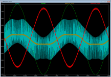
pictures are a discrete power comparator and normal output stage switching on 700 Khz or around.
The class D in picture schematic is with a multi pole HD shaper.
Succes with the attemps, I go follow this.
Class D is shure nice play tools, but wauw so much attemps to get the best amp, still there is room for patents.
pictures are a discrete power comparator and normal output stage switching on 700 Khz or around.
The class D in picture schematic is with a multi pole HD shaper.
Succes with the attemps, I go follow this.
Attachments
Check this for OCP test:
https://www.youtube.com/watch?v=r5k0uWBQogk
The OCP for D2KNeo is made by me. I like simple and well proven.
I see someone asking OCP for discrete LTP, the schematic in the first page. I can make it if it is still required.
https://www.youtube.com/watch?v=r5k0uWBQogk
The OCP for D2KNeo is made by me. I like simple and well proven.
I see someone asking OCP for discrete LTP, the schematic in the first page. I can make it if it is still required.
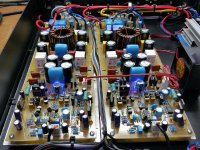
And this is my discrete UcD.
Of course it is with protection.
Please post all details,pcb and schematic for this amlifier.
I want to built my second class D.
Kees,
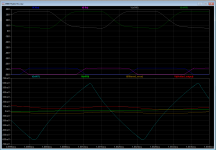
Nice, but I don't understand some things. Why do you call the 1st one digital? If timing was discrete only then it was digital. Why switching freq changes asymmetrically, and why do you accept it? What "HD" stands for? And please adjust window size of FFT to whole periods to avoid spectral leakage!
About the second sim:
Hysteretic ucd is an oximoron. UcD is free of hysteresis (check in patent!). And doesn't use pre-filter feedback at all. And why to mention 2nd harmonic in a basically symmetric circuit when there is a 30 dB bigger 3rd harmonic?
Generally: to design a practically useful schematic there are further requirements above switching freq and distortion:
- Low idle loss and low distortion at small signal (these are contradictional requirements!)
- Low loss at nominal power.
- Low output offset voltage with unmatched components
- Acceptable temperature dependency of the above mentioned parameters (may be checked with temp parameter stepping)
- Low sensitivity to parasitic effects
- Good overdrive behaviour
- Safe turn on and off behaviour
- Stable and safe operation without load
- Fast overcurrent protection
- Overvoltage protection
- Stable and safe operation without input source
- ...
Last edited:
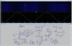
Let show my circuit.
It is:
- Low idle loss and low distortion at small signal (these are contradictional requirements!)
- Low loss at nominal power.
- Low output offset voltage with unmatched components
- Acceptable temperature dependency of the above mentioned parameters (may be checked with temp parameter stepping)
- Low sensitivity to parasitic effects
- Good overdrive behaviour
- Safe turn on and off behaviour
- Stable and safe operation without load
- Fast overcurrent protection
- Stable and safe operation without input source
Sorry no overvoltage protection required for me, as my experience, pumping effect is less than 10% nominal.
Bonus: DC Protect and Front Signalling.
Sorry no PCB for share.
Attachments
- Home
- Amplifiers
- Class D
- UCD 25 watts to 1200 watts using 2 mosfets