I will maybe change that but with the predriver there will be an additional vgs drop of 1 - 2V and with the predriver the higher value will not be a problem.
Last schematic before PCB. 😉
Hi Sonnya
For the testing purposes schematic is OK, but casoded Sziklai compounds and enhanced rails nested CCS-s were used in the first place to eliminate the need for extra CCS-s, which therefore don't legitimate their presence. Measurements will clearly show if the ratio of benefit vs. unnecessary extra complexity would be justified. In the same manner we can think about using DC servo. 🙄
Anyway, I hardly wait to see the PCB layout
Thats why i have added solderjumps to the ccs bias circuit
Thats why i have added solderjumps to the ccs bias circuit
Yes I saw that too.

And there is still possibility no to use Sziklais than these could come handy.
Please say something more about PCB, maybe dimensions, layers, etc. Thanks Sonnya 😉
Last edited:
Yes I saw that too.
And there is still possibility no to use Sziklais than these could come handy.
)
?? Could you explain?
As far as i understand Lazy Cat he thinks that your bias arangement is obsolete when we use the Fet Cascoded Sziklay ( FCS ).
I know that. I could easily remove it from the circuit.
And pass all data on to you.
I do not believe it is a good idea to have bias difference in the parts of the circuit taking care of all the work (i.e. feedback) because that we want to set offset and idle current.
I see no point in building it from my point of view, when this part is not present.
As i have made it, it can always been disabled.
Sonnya you've said that you want the input bias to be independant of output bias setting, because using only master bias trimmers for both, would cause different and uncertain sonic signature, without possibility to find a sweet spot for each of them. With introducing Sziklais in TSSA Basic, bias current in input gain transistors is fixed by Vbe/Rbe, in that way we simply avoid the need of separate bias settings (input bias is fixed in this case) and master bias/offset trimers in pos/neg CCS would be just fine.
You also mentioned that maybe, bacause of better sound, Sziklais will be omitted later, and only cascoded input pair would be present. For this situation your separate bias/offset CCS-s would again be needed to enable independant bias setting for both stages.
Hopefully you find my explanation to be satisfactory, regards Andrej 😉
Did i say that i want to remove it ? No !
You and me are the only ones that build this animal. I say that this is such a different toplogy that we really have to study this in detail. Even it´s creator may not understand it 100 %. Art comes before science because intuition is faster then understanding. I think that is where LC is really good at.
You and me are the only ones that build this animal. I say that this is such a different toplogy that we really have to study this in detail. Even it´s creator may not understand it 100 %. Art comes before science because intuition is faster then understanding. I think that is where LC is really good at.
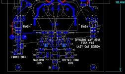
First layout - placement
Back side of PCB will be mainly GND plane.
PCB looks great, Sonnya 😎
Dual layer PCB also enables the SMT parts to be mounted in bottom layer below regular parts mounted on top layer. In that case we have possibility to significanly reduce PCB size, traces lenghts, etc.
- Home
- Amplifiers
- Solid State
- TSSA - The Simplest Symmetrical Amplifier