Hello,
Got a new marantz sitting on my table but the main amp board is in pretty bad state, it's obvious one or more failed attempts to fix it have been made, a lot of tracks are missing and were poorly repaired, some resistors had been replaced but soldered in series in stead of both connecting to earth, some transistors only had one or two legs soldered to the board and 4 of the 8 power transistors that had bee replaced with BD911/912 pairs are shorted (one entire channel). The pre drivers and drivers have alson been replaced with MJE15031/15030 for the drivers and MJE 340/350 for the pre-drivers (those are fine but are they good replacements here ?
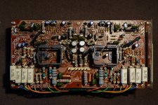
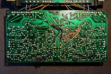
My actual question is what would be the best substitutes to the original 2SB618/2SD588 power transistors ?
There also are some MV-1 that seem a little dodgy, any way to replace those with common diodes ?
Got a new marantz sitting on my table but the main amp board is in pretty bad state, it's obvious one or more failed attempts to fix it have been made, a lot of tracks are missing and were poorly repaired, some resistors had been replaced but soldered in series in stead of both connecting to earth, some transistors only had one or two legs soldered to the board and 4 of the 8 power transistors that had bee replaced with BD911/912 pairs are shorted (one entire channel). The pre drivers and drivers have alson been replaced with MJE15031/15030 for the drivers and MJE 340/350 for the pre-drivers (those are fine but are they good replacements here ?


My actual question is what would be the best substitutes to the original 2SB618/2SD588 power transistors ?
There also are some MV-1 that seem a little dodgy, any way to replace those with common diodes ?
OK so finally I decided to go with some new BD911/912 and everything seems to work fine, I'm able to get a DC offset of about 5mV and I get a beautiful sine wave on the speaker terminals but the problem is that I only have 3mV idling current on one channel (between the emitters of both pairs of pnp/npn) and 9.5mV on the other channel. The service manual doesn't give any info on what the bias should be and there is no adjustment possible. Are these values too low and too unbalanced between both channels or is there no need to worry ?
Obviously the 911-912 combo is slower than the original and a bit lower voltage ,,,,Obviously also it doesn't turn on the same way like the Japanese cousins do so that is why you cannot bias it properly ...
I could consider a repair like that as a degrade ...
here is my two cents ...
Practice like that originates from the obsession of a few manufacturers to use the specific NEC transistors ( pretty fast all of them but in reality SOA was very poor ) There was a time that every Japanese amplifier was made with them ..Gave up though within a few years when SOA problems arrived....NEC was blown way too easily ...
To produce 75W one pair wasn't enough so they needed two pairs but in most of cases much of the signal was lost in the interference and the extensive wiring between the 4 transistors Remember also that at the time most pcb was hand drawn and there was no clever idea on how to design a PCB to achieve minimal wiring between the 4 transistors ..Not to mention that most cooling ideas originated from TO3 transistors and that was a problem ....
so what you really have to do is correct that mistake instal Just a pair of 1943 5200 or 21193 -4 simplify the wiring and play with Vbe to manage the bias ...In the end you will have a far better amplifier safe rugged and playing very well....
This a choice that i have done in the past in similar models since transistors was obsolete and worked surprising well . Now days i have transistors ( again) but i only install them in smaller circuits that use only one pair and only if the costumer is willing to pay for an original ....( got the drivers also ) ......
Kindest regards
Sakis
Last edited:
I would fit the originals. Donberg have some; Semiconductor: 2SB618 (2SB 618) - TRANSISTOR SILICON PNP / 150V / 7A / 80W / 14MHz...
Hi! Jonsnell,
Problem is they are 20€ a piece and there are 8 of them to change. East eletronics' idea seems more afordable and could actually be an improvement. When doing this though shoumd I Just leave the resistors used for the second pair of transistors or get them out of the board ?
When you say they are slower I suppose you refer to the switching frequency. The original nec transistors were at 7Mhz and the fairchild bd's are at 3Mhz, is there a minimum to avoid crossing in this type of use or does that depend on the design of the rest of the amplifier ?
Hi Sakis, finally received my parts today and am starting to redesign the output stage to fit only one pair of complementary transistors per channel. Can I just remove 1 pnp and on npn on each channel and their corresponding emitter resistors or is it a little more complicated than that ?
here are the schematics with the corresponding tracks connected to each transistors I'm going to remove.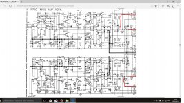
here are the schematics with the corresponding tracks connected to each transistors I'm going to remove.

I made a mistake on the schematics, on the upper side it's J717 and J719 that I will remove and not J711 and J719.
I followed your advice and bought 2 pairs of 2sa1943/2sc5200. So I removed 2 pairs of the original transistors (1 on each channel). these correspond to the wires connecting to J717 and J719 on one channel and J718 and J720. For the 2 pairs that I removed, can I just also remove the 2 corresponding emitter resistors and leave all the rest as is (except for the vbe that will have to be modified) ?
sorry i am not with you at this point
If you have one amplifier with 4 small transistors in the output that are unobtainable then you need to remove them all ( all 4 of the old ones ) install just a pair of bigger transistors drive them from the same base signal that existed in the past use emitter resistors exactly as the old ones, maintain the same value for the resistor replace though if the old ones are 2W types with 5W types
bias , check for offset, oscillation ...done
Ok It's not explained the same way but we're on the same page 😀.
Now there are 4 emitter resistors per channel and I just wanted to know if I could remove the 2 that aren't necessary any more as I now have only one pair.
You gave me an answer without knowing it so thanks. I don't have micas for these cases and will have to get some more powerful emitter resistors so it might take some time before my nest update.
Depaj
Without knowing much about you ( i actually dont know your depth of knowledge or the instruments you have )
A few things more
You will probably need to recalculate the VI limiter and change the sensitivity accordingly
The amplifier features a VI limiter so there is a very good chance that it kicks to fast killing the sonics or work ineffectively to protect the amplifier correctly .
Scope will be needed here i estimate that you know that ....
Kindest regards
Sakis
Okay, I think you're getting close to some of my limits, redesigning part of an amp has not been on my program so far but this is exciting 🙂, I will need some guidance though !!
So I will have to recalculate the power limiter to protect the output transistors right ? And I will have to use a scope to check for clipping. I think I got that part but then, how exactly will I have to calculate this and what are the components I need to adjust to get there ?
Second part, usually I don't have any trouble finding the vbe but this time is different, would it be ok to just replace a fixed resistor by a trimmer to adjust bias and if yes which one ?
Last edited:
not really
The scope is going to be needed to look if there is any oscillation, clipping conditions also but under a variety of loads ...
You need to have and use a variac or at least a bulb tester to power up first , monitor bias see if its too much or too little and work accordingly ...
yes ...in reality overload protection should be calculated in order to meet the SOA of the new transistors ( you will find plenty of calculation forms in the forum all limiters of this type work on the same principal IE monitor voltage drop on emitter resistors activate one small transistor per rail to shunt the drivers to output when load increases )
Last edited:
I'll have to go with the bulb tester, don't have a variac yet.
This will have to wait till I get the isolators,I don't want to risk overheating the ouputs if something goes wrong. And I won't be able to work on it for a couple of weeks. I'll let you know when I'm back, thanks for all the precious help so far 🙂.
This will have to wait till I get the isolators,I don't want to risk overheating the ouputs if something goes wrong. And I won't be able to work on it for a couple of weeks. I'll let you know when I'm back, thanks for all the precious help so far 🙂.
I could still use some help on how to calculate the overload protection, this is something new to me ! I've been looking for these forms you told me about but couldn't find anything (at least not clear enough for me to understand.
This is the datasheet for the new output transistors I installed, how do I proceed to calculate and how do I translate this into the actual values needed in the circuit ?
View attachment SOA 2SA1943.pdf
And this is the main amp circuit
View attachment main amp marantz 1122dc.pdf
This is the datasheet for the new output transistors I installed, how do I proceed to calculate and how do I translate this into the actual values needed in the circuit ?
View attachment SOA 2SA1943.pdf
And this is the main amp circuit
View attachment main amp marantz 1122dc.pdf
Hello again,
Just finished installing the new output transistors and powered up the amp with a bulb tester. Relay closed after a while (a little longer than usual). I measured the offset and managed to set it to around 3mv but it isn't very stable (it goes up again every time I switch the amp off and on again). I have around 10mV of bias on one channel and 22mV on the other. So far I haven't changed the emitter resistors yet, should I just remove the pair that was connected to the second pair of outputs that I removed and replace the other pair by same value resistances but higher power dissipation resistors or do I need to change value as well ?
For the vbe I would like to install two trimmers to be able to adjust it precisely. there are two transistors in the bias circuit per channel (Q720 (721) and Q723 (724)) where would be the best place to put those trimmers ?
Ok so I replaced the emitter resistor with more powerful ones and started testing, relay clicked and the d offset stabilised around 0mV. I get 22mv bias on the right channel and 11mv on the left channel. Both test ok with a 1kHz signal and no load. When I connect a dummy load (8ohm 100w) to the right channel, no problem, nice clean sine wave and the amp stays stable but when I do the same with the left channel the bulb tester lights up quite brightly as soon as I turn up the volume and the amp goes nuts (oscillates between +/- 1v) and I have to power off.
I haven't had any answers for a while, anyone ??? Thanks
I haven't had any answers for a while, anyone ??? Thanks
Last edited:
Haven't really done anything to it these last days but today I fired it up again and did some tests with 8 ohm dummy loads and everything seems fine, got a beautiful and equal sine wave on both sides. Still I got around 6mV of bias on 1 side and about 24mV on the other, The vbe seems to be set by diodes so no way to adjust, is there anything I can do to get a proper bias on both channels (the drivers heat sinks are getting quite hot on both sides).
Also the manual says : rated power at 1kHz into 8ohms 76W two channels driven. That is exactly what I get when taking P : Umax² / 8 but when I use Ueff I only get 39W. Is the power stated in the manual obtained by using the first method or don't I get the power output that I should get ?
Also the manual says : rated power at 1kHz into 8ohms 76W two channels driven. That is exactly what I get when taking P : Umax² / 8 but when I use Ueff I only get 39W. Is the power stated in the manual obtained by using the first method or don't I get the power output that I should get ?
- Status
- Not open for further replies.
- Home
- Amplifiers
- Solid State
- transistors Marantz 1122 dc