This is correct, but then you'd skip this ADAU and go for one without internal ADC/DAC section.
(Possibly with internal SRC and SPDIF-Receiver)
They layout/implementation is from late 2014/early 2015, at this time i had no clue that PCM51XX/52XX exists.
50Mips is not a deal-breaker, you can do alot of math/stuff if running at "low-spec" 48kHz. Haven't hit the instruction limit with my actual implementation, which consists of:
DC-Blocking
Stereo2Mono
2-Way X-over + shelving EQ
Some kind of Maxbass
selectable EQ Presets via external Buttons
selectable Loudness compensation via external ADC + Potentiometer
2 Band Compressor/Limiter
3 LED level indictator with S&H
36dB subsonic
Having 98% of my source-material in 44.1/48kHz and/or MP3/AAC, why would i spend money/ressources on 32/384 just because i can? I also have some 24/96 lossless content, but would i hear a difference between 24/96 and 32/384? 😉
You can route from DIR/AES to the PCM5102 with SRC/ADAU bypass and still have the audio mixed in this implementation here, also at rates the ADAU does not support.
The actual implementation can be configured as:
ADAU + SRC4382 + PCM5102
ADAU + SRC4382 only
ADAU + PCM5102 only
ADAU only
So if someone just need an analog 2-way stereo x-over, this can be build - Analog 3-way stereo x-over, yep. 😀
Btw, the MiniDSP Core within the PCM5242/5142 also run at "only" 48kHz:
So pretty much the same as the small ADAU DSPs. Want more? Go for "sharkDSP".
(Possibly with internal SRC and SPDIF-Receiver)
They layout/implementation is from late 2014/early 2015, at this time i had no clue that PCM51XX/52XX exists.
50Mips is not a deal-breaker, you can do alot of math/stuff if running at "low-spec" 48kHz. Haven't hit the instruction limit with my actual implementation, which consists of:
DC-Blocking
Stereo2Mono
2-Way X-over + shelving EQ
Some kind of Maxbass
selectable EQ Presets via external Buttons
selectable Loudness compensation via external ADC + Potentiometer
2 Band Compressor/Limiter
3 LED level indictator with S&H
36dB subsonic
Having 98% of my source-material in 44.1/48kHz and/or MP3/AAC, why would i spend money/ressources on 32/384 just because i can? I also have some 24/96 lossless content, but would i hear a difference between 24/96 and 32/384? 😉
You can route from DIR/AES to the PCM5102 with SRC/ADAU bypass and still have the audio mixed in this implementation here, also at rates the ADAU does not support.
The actual implementation can be configured as:
ADAU + SRC4382 + PCM5102
ADAU + SRC4382 only
ADAU + PCM5102 only
ADAU only
So if someone just need an analog 2-way stereo x-over, this can be build - Analog 3-way stereo x-over, yep. 😀
Btw, the MiniDSP Core within the PCM5242/5142 also run at "only" 48kHz:
The miniDSP can run up to 1024 instructions on every audio sample at a 48kHz sample rate.
NOTE
At higher sampling frequencies, fewer instruction cycles are available. (For example, 512 instructions can be done in a 96kHz frame.)
So pretty much the same as the small ADAU DSPs. Want more? Go for "sharkDSP".
Last edited:
Oh yeah, I fully understand it is 100% pointless, possibly even detrimental, as the best source material I have is 24/96 for a few albums, and mostly 16/44.1 or MP3.
I am only just starting to experiment with DSPs so I have no idea what I really need just yet, but I know I probably don't really need even 50 MIPS in reality based on other products I have looked into. That said, when it comes to hardware, I typically take the Binford approach, which is to say, MORE POWER! (sorry, if you don't get the reference, look up "Tool Time" 🙂 )
I did realize after my post that this project has been going for you for awhile and the 5x42 are the newest ICs.
The ADAU1451/52 look like a nice beefy DSP/ASRC/SPDIF Transceiver. They will not do 384kHz, which is fine. They will do 32 bit though, and I do care some about that, for better digital volume control. Plus 294 MIPS 🙂
Anyway, back to the TPA3251, I have ordered the parts to populate the two red boards I have with the 3251 IC. I hope to have at least one them done either first or second weekend in May, looking forward to hearing what the bigger TPA IC's have to offer.
I did at first, but then I read the datasheet and realized that I will only pick up 10W (50W up to 60W, both before the distortion threshold) into an 8R load anyway, so not a big improvement. So I will run it in standard BTL for awhile. I will probably want to give PBTL a shot at some point, but no rush, for now I can enjoy it into twice as many speakers 🙂
Off topic:
I got some time to work on my layout and I have a quick question.
When routing the audio line-in signal, should I keep the signals the same length? Am I wasting time and creating unnecessary interference since this is not digital signal pair? This is extremely time consuming to do in EAGLE. 😛
I got some time to work on my layout and I have a quick question.
When routing the audio line-in signal, should I keep the signals the same length? Am I wasting time and creating unnecessary interference since this is not digital signal pair? This is extremely time consuming to do in EAGLE. 😛
Attachments
Off topic:
I got some time to work on my layout and I have a quick question.
When routing the audio line-in signal, should I keep the signals the same length?
Impedances with low level audio signals are usually pretty high so the difference in resistance between small differences in trace length have very little impact. The frequency range required by audio signals is very small too (realistically 20kHz small) so parasitic inductances and capacitances have next to no effect on the audio signal.
The only thing you'd have to watch out for is if the silicon you're connecting to (or from) could be made unstable by parasitics, but measures can usually be taken to make these a non-issue if necessary.
On another note if you're using balanced signals it's usually best to run the lines as parallel to one another as you can, but again, you don't need to do anything crazy like match lead lengths - at least not in my experience of building equipment and measuring for specified performance.
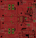
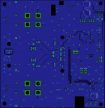
Hello all,
I finally got the layout in a satisfactory state (4th revision), but I want to see if you guys can spot any show stoppers/problems that I missed before I send it off. This is my first layout of a board dealing with high power and this many components so I have some doubts.
I did these things:
- Kept decouple caps close to their respective IC's with low impedance traces.
- Routing differential signal together where possible. I do not plan to use DIFF.
- Used Saturn PCB calculator to make sure traces width and via sizes will handle current with 1°C temperature rise.
- Avoided sharp corners. I think this has little purpose because fs is only 600kHz.
- Passed DRC of board manufacturer.
I am not sure about:
- Ground planes broken up in some places. Will this cause problems?
- Will current loops cause major problems? My routing is not on par...
- I have a 12V trace routed underneath the tpa3251 on the bottom plane. Will this cause problems?
- Bootstraps for OUT_B and OUT_C is not routed optimally. Should I redesign?
- Supervisor circuit is kind of far away from the tpa3251. Will this effect functionality of the circuit?
This layout is far from perfect, performance not top priority. I just want to have a reasonable expectation that this board will work when I put it together. I am learning and I really appreciate the help. 🙂
Thank you for your time and critique.
Attachments

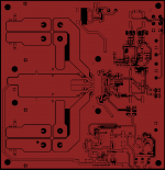

Difficult to say without schematic... Looks like a reasonable layout and will probably work (if the schematic is correct).
Boost traces are not so critical.
You probably noticed the TI eval board puts all the output traces on the bottom side and solid ground on the other side, this gives somewhat lower EMI when the amp is mounted in a metal case as the output traces cannot radiate to the cabling then. For DIY is probably not an issue.
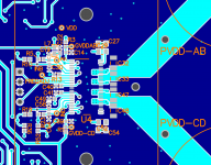
Some things noticed:
- In the left-lower corner, there is a trace very close to the mounting hole.
- Seems the lower side of the heatsink clashes with a power regulator and a capacitor. The capacitor is obvious, the power regulator might be too thick to fit under the heatsink which is less obvious.
- Wondering if the vol pot really fits, it's very close to the capacitors.
- Routing around the opa's input looks a bit long + left / right too close (cross talk possible). If you use high bandwidth opa's, it might lead to instability.
- Depending on the DC output bias of the opa's, the capacitors between the opa's and the TPA might have the wrong polarity. Don't use a very high capacitor value here, otherwise you might blow the inputs of the TPA when switching on, depending on the opa's supply voltage. (don't ask how i know this...)
Rob
Boost traces are not so critical.
You probably noticed the TI eval board puts all the output traces on the bottom side and solid ground on the other side, this gives somewhat lower EMI when the amp is mounted in a metal case as the output traces cannot radiate to the cabling then. For DIY is probably not an issue.
Some things noticed:
- In the left-lower corner, there is a trace very close to the mounting hole.
- Seems the lower side of the heatsink clashes with a power regulator and a capacitor. The capacitor is obvious, the power regulator might be too thick to fit under the heatsink which is less obvious.
- Wondering if the vol pot really fits, it's very close to the capacitors.
- Routing around the opa's input looks a bit long + left / right too close (cross talk possible). If you use high bandwidth opa's, it might lead to instability.
- Depending on the DC output bias of the opa's, the capacitors between the opa's and the TPA might have the wrong polarity. Don't use a very high capacitor value here, otherwise you might blow the inputs of the TPA when switching on, depending on the opa's supply voltage. (don't ask how i know this...)
Rob
Having some series resistance within the lines should avoid this (like 1k).Don't use a very high capacitor value here, otherwise you might blow the inputs of the TPA when switching on, depending on the opa's supply voltage. (don't ask how i know this...)
Well, nice idea, but these calculations are for steady DC. You can relax on this when just using the RMS values. While having 1°C in mind, even 10°C wont hurt.Used Saturn PCB calculator to make sure traces width and via sizes will handle current with 1°C temperature rise.
Notes:
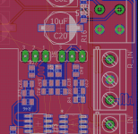
- The bulk cap mounting holes look a bit small in diameter
- Consider to have your input terminals mechanical linked together, that's why they have those small "noses" + slots
- The input of your buck isn't optimal but may work for that low currents you have
- Is this Buck-IC is without thermal pad?
Of course, the output caps of the buck needs to be mounted differently (like 180°) to have the copper pours work.
FYI:
Attachments
Last edited:
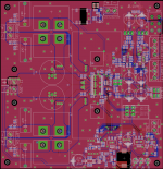
Hi trashcanz,
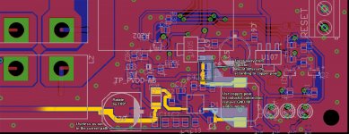
The biggest concern I have about this layout is the GNDpin-CAP-PVDDpin loop area for the PVDD decoupling caps C32, C33, C47 and C48. It looks like quite a long inductive path from the GND side of the caps back to the IC pins, particularly because current needs to go through 2 sets of vias before getting back to GND. This will cause higher ringing and spikes, possibly damaging the IC at high power. See TI EVM layout (fig 3):
http://www.ti.com/lit/ug/slvuag8a/slvuag8a.pdf
The TI EVM keeps this decoupling path very short, and keeps it all on the topside
Rob,
Thanks for spotting the capacitor underneath the heatsink! It must of shifted in there while I was trying to downsize the board. The regulator should have clearance but I moved it out just in case.
I do not plan on soldering the pot on board but it should fit the pot I am using.
I tried moving the left/right signal as far as possible to avoid crosstalk. Routing length and clearance wise is not too good due to the way I arranged the headers.
The schematic was mostly lifted from the EVAL board with some doctormord additions. The capacitors are 10uF and I will also put a 1k resistor in series with the inputs when needed.
Doctormord,
Thank you again for the suggestions. I have made the changes you have listed. The graphics were very helpful. The Buck-IC does not have thermal pad.
Frammis,
Thanks for bringing this to my attention. I have redesign the OUTs a bit. While it is still not optimum, I think it has addressed this issue.
Hopefully, I have implemented the suggestion you guys have made correctly. I can not thank you enough for your replies and your time! 😀
Attachments
Last edited:
I completely forgot that I was going to keep the output traces on the bottom of the board from the TPA to the speaker terminals instead of going down and back up again. Seems like a much more reasonable way to do it like you guys suggested. Too tired, worked on this overnight and it is almost sunrise.
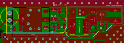
Hmm, still not happy with the buck. Why there is so much parallel MLCC before the ferrite? How much current demand is on that rail? What frequency range are you trying to decouple there?
The ground-return loops are still large -> via stitching is not optimal there. Every current on the rail will have a corresponding ground path under trace which will narrow with rising frequency.
Rule of thumb, every capacitor gets its own via stitched to GND as close as possible to the pad. 0805 and up will have 2. Have then orientated to the IC.
Suggestion. Put 2 of the 4 MLCCs right beside the (input) diode, 90° rotated with GND to the buck ic. Remove the other 2. Move the bulk cap close to the diode then. Add 10n 0402 behind the diode close to the input pin of the buck-ic. Put 2 Vias under the IC stitched to GND.
Get the current loops as tight as possible there.
Beside this, you should get rid of the track right under the 3251, which cuts your plane.
Are you going to have a pinheader right "in" the heatsink?
Isn't this buck-ic a LM5010? Then there's a thermal pad for sure.
Last edited:
Rob,
Frammis,
Thanks for bringing this to my attention. I have redesign the OUTs a bit. While it is still not optimum, I think it has addressed this issue.
Hopefully, I have implemented the suggestion you guys have made correctly. I can not thank you enough for your replies and your time! 😀
Hi trashcanz,
Good improvement- The decoupling loop ground return looks much better for Cap C33 to GND pins 25,26 and for C48 to GND pins 41,42. I don't think caps C32 or C47 are doing much to help (usually paralleling same values of MLCC's hurts more than helps due to slight offsets in self resonance). These extra 2 caps were intended to decouple PVDD to GND for the center 2 half bridges to GND 33 and 34. Unfortunately, the inner ground pins (33,34) are "trapped" by the output traces. What TI did on the EVM was to via the middle 2 outputs down to the bottom layer to untrap the GND pins. See attached, Top & Bottom views.
Attachments
The TI datasheet is a bit unspecific which GND pin belongs to which h/half-bridge. Maybe they fix this in a revision.
(Actually there isn't any datasheet available?)
(Actually there isn't any datasheet available?)
Hi Dr Mord,
I saw that weird thing of the missing datasheet for TPA3251D2 on the TI website today. I sent feedback to the webmaster to see if they can fix it.
I saw that weird thing of the missing datasheet for TPA3251D2 on the TI website today. I sent feedback to the webmaster to see if they can fix it.

- Home
- Amplifiers
- Class D
- TPA3251d2