Simulating Thermal-Lag in the MOS-diodes
Hi Pawel,
Sorry, my last post subcircuit was forgotten in the zip. The missing ones are in the latest one below.
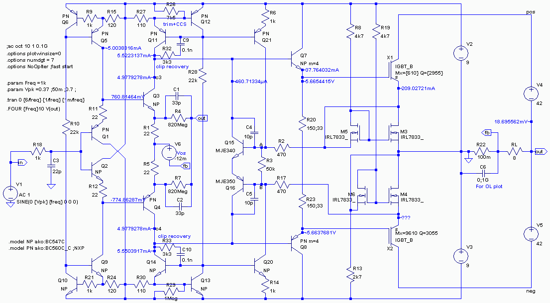
This one shows heating up from idle with 40W, then change at 10s to 1W and it cools. It is the version for 8 ohms and includes electrothermal models for the main MOSFETs and the MOS-diodes (4 MOSFETs). Sorry about the clutter from the thermal model bits. M4 is coupled to M3 via Ts3 label, likewise M6 is coupled to M5 via Ts5 label, and M3 and M5 are not thermally coupled (but the could be linked by changing the labels). The thermal resistance for cooling M3 and M4 is 50C/W, assumed to be that of two TO-220's coupled together.
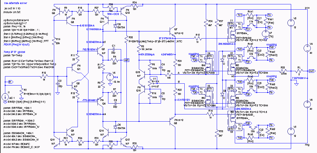

.
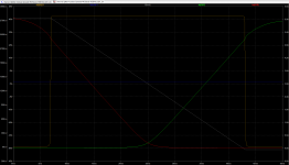
This show the thermal time constants in the main MOSFETs and the MOS-diodes. The idle current (t=0) is 295mA, t=1s is 318mA, t=10s is 347mA, t=11s is 325mA, t=20s is 301mA.
With 40W, once the heatsink reaches final temperature the crossover current is 50mA more than at idle, the HS rise is 17C from idle. About half the current change occurs in the first second.
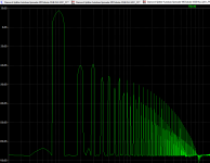
The FFT was plotted for the first 5 cycles from t=0, 1s, 9.5s, 10s, 11s, 20s. There is a check box for the in the FFT dialog.
At t=0 40W the dominant harmonic is -70.9dB, then at t=9.5s it is 70.8dB so the increase in idle current is not causing more distortion.
At t=10s 1W the dominant harmonic is -98.5dB, then at t=20s it is 93.7dB so the increase in idle current from 40W reduces the distortion compared to after the heatsinks cool back to their normal idle current of 295mA. This is because an idle current of 295mA is "under-biased", deliberately to reduce the idle heat to a "reasonable" level.
BTW The "optimum" idle current for this output stage is relatively high because there are effectively no source resistors (the MOS diodes have only about 20m Ohms of resistance, much less than the usual 200-300m Ohms.)
In this simulation I have used guestimate values for the thermal properties of the MOS-diodes. They are not on a heatsink, just back-back with a thermal pad. Once bench measurements are made the thermal linkages can be updated for real life simulations. In the mean time we can see the general effects such as thermal lag in the MOS-diodes and the effect on distortion.
BTW D1 and D2 are added across the MOS-diodes so LTspice can find the correct operating point. They do not normally conduct in this circuit and are (probably) not needed in a real circuit.
Hi Pawel,
Sorry, my last post subcircuit was forgotten in the zip. The missing ones are in the latest one below.
This one shows heating up from idle with 40W, then change at 10s to 1W and it cools. It is the version for 8 ohms and includes electrothermal models for the main MOSFETs and the MOS-diodes (4 MOSFETs). Sorry about the clutter from the thermal model bits. M4 is coupled to M3 via Ts3 label, likewise M6 is coupled to M5 via Ts5 label, and M3 and M5 are not thermally coupled (but the could be linked by changing the labels). The thermal resistance for cooling M3 and M4 is 50C/W, assumed to be that of two TO-220's coupled together.
.
This show the thermal time constants in the main MOSFETs and the MOS-diodes. The idle current (t=0) is 295mA, t=1s is 318mA, t=10s is 347mA, t=11s is 325mA, t=20s is 301mA.
With 40W, once the heatsink reaches final temperature the crossover current is 50mA more than at idle, the HS rise is 17C from idle. About half the current change occurs in the first second.
The FFT was plotted for the first 5 cycles from t=0, 1s, 9.5s, 10s, 11s, 20s. There is a check box for the in the FFT dialog.
At t=0 40W the dominant harmonic is -70.9dB, then at t=9.5s it is 70.8dB so the increase in idle current is not causing more distortion.
At t=10s 1W the dominant harmonic is -98.5dB, then at t=20s it is 93.7dB so the increase in idle current from 40W reduces the distortion compared to after the heatsinks cool back to their normal idle current of 295mA. This is because an idle current of 295mA is "under-biased", deliberately to reduce the idle heat to a "reasonable" level.
BTW The "optimum" idle current for this output stage is relatively high because there are effectively no source resistors (the MOS diodes have only about 20m Ohms of resistance, much less than the usual 200-300m Ohms.)
In this simulation I have used guestimate values for the thermal properties of the MOS-diodes. They are not on a heatsink, just back-back with a thermal pad. Once bench measurements are made the thermal linkages can be updated for real life simulations. In the mean time we can see the general effects such as thermal lag in the MOS-diodes and the effect on distortion.
BTW D1 and D2 are added across the MOS-diodes so LTspice can find the correct operating point. They do not normally conduct in this circuit and are (probably) not needed in a real circuit.
Attachments
An observation... whats is so bloody special about 20kHz? A lot of circuits you see start to drop of FR wise or has a rising presence of distorsion around 10k.. Is this just a coincident or is it dues to our 20-20k thinking that make it end up like this.... But its not all in our minds - there seem to be som sort of physical limit also that kicks in. Most class-d has a dist jump at 7-9 k. Regulators start to keep the grip (output impedance etc) at 10k.
Why isn't this figure 63k instead so it could be well outside our pass band?
//
Why isn't this figure 63k instead so it could be well outside our pass band?
//
It could be 63KHz. You would need less gain. Gain is a function of impedance. Higher gain, higher impedance and parasitic capacitance determines bandwidth. Operating at higher currents in signal stages is a way around this but leads to higher distortion.
That is why open loop gain drops with frequency, which reduces feedback and causes distortion rise.
That is why open loop gain drops with frequency, which reduces feedback and causes distortion rise.
I think I do know this but I'm so psyched that the limits seem to coincide with the human hearing boarder - why isn't physics just 10x better and we would not have any problems... really 🙂
//
//
Simulating Thermal-Lag in the MOS-diodes
In addition I have added thermal compensation so the idle current remains more constant with the main MOSFET temperature changes, particularly from startup. R10 is now a 22k thermistor mounted on M1 case. It is optional.
Oops. There was a mistake in the signal source😱. The corrected file is attached for the stated power changes. My apology.Hi Pawel,
This one shows heating up from idle with 40W, then change at 10s to 1W and it cools.
In addition I have added thermal compensation so the idle current remains more constant with the main MOSFET temperature changes, particularly from startup. R10 is now a 22k thermistor mounted on M1 case. It is optional.
Attachments
Autobias versions
Hi All,
Here are the autobias versions for BJT and MOSFET power transistors (below):
.

.
What's changed? The spreaders (Q15,Q16) now have current sources for setting their operating point rather than the feedback resistors used in a Vbe multiplier (see Post 83 above R6,R16).
To get the autobias to cover the full output current range several CCS conditions need to be met. Q15,Q16 are operated at 100uA by R6,R14. Then R3 and R14 are chosen for the idle current. Then R28 and R30 need to supply the same current as to the input stage (Q5,Q9) plus the 100uA to the spreaders.
Also, to get autobias to cover the full output current range the minimum idle current depends on the choice of MOS-diodes; the lower their Ron the lower the minimum idle current. For the MOS-diodes used here the minimum idle current to cover the full output current range is about 200mA (for about 38V peak or close to 100W into 8 ohms).
When the CCS balance conditions are met the MOSFETs can be swapped for BJTs (and once the base-emitter resistors are lowered and the compensation is changed to suit the BJTs) then the autobias circuit automatically gives about the same idle current -- and that's without altering the CCS balance😎. And notice there's no trimpot for the spreader (which was a Vbe multiplier but now an autobias loop).
The MOSFET and BJT versions are in the attached files so you can see the idle currents are about the same for the BJT version as for the MOSFET version without changing the CCS balance conditions and without a trimpot.
In a practical version of this amp there will probably need to be a trimpot somewhere to get the CCS balance about right. But there doesn't seem to be any need with this autobias amp to operate at an optimum idle current for minimum THD because the wingspread curve is fairly generic and fairly insensitive to the idle current.
The main requirement is to get the autobias to cover the full output range so it doesn't create a sudden gain change (near full output swing) if the common-mode feedback for autobias loop stops. But we knew autobias is living dangerously😀 (see Post 1 an a few of the early posts).
A few performance figures for this autobias version:
BJT version f-3dB 1MHz, MOSFET 2MHz (as per attached files).
SR both 38V/us and OK to 200kHz full output with no cross-conduction and above 200kHz the crossover collapses (which is nice and safe😎).
THD at 1kHz 50W 0.04% BJT and MOSFET 0.013%.
THD at 1W 0.005% BJT and MOSFET 0.007%.
Idle current and THD don't change much with ambient or power transistor junction temperatures.
This provides, after a fairly long journey, a wideband autobias topology that is not overly complex.
Admittedly it's a bit tricky to set up the CCS operating point but it's early days. After building several amps we may find the best way to get it to work first try. Here's for hoping😉.
BTW the above amp is configured for current drive amp with R22 in series with the load for feedback and with R4 and R7 disabled.
For a voltage drive amp short this resistor and reinstate R4 and R7 back to 820 ohms.
Cheers,
Ian
Hi All,
Here are the autobias versions for BJT and MOSFET power transistors (below):
.
.
What's changed? The spreaders (Q15,Q16) now have current sources for setting their operating point rather than the feedback resistors used in a Vbe multiplier (see Post 83 above R6,R16).
To get the autobias to cover the full output current range several CCS conditions need to be met. Q15,Q16 are operated at 100uA by R6,R14. Then R3 and R14 are chosen for the idle current. Then R28 and R30 need to supply the same current as to the input stage (Q5,Q9) plus the 100uA to the spreaders.
Also, to get autobias to cover the full output current range the minimum idle current depends on the choice of MOS-diodes; the lower their Ron the lower the minimum idle current. For the MOS-diodes used here the minimum idle current to cover the full output current range is about 200mA (for about 38V peak or close to 100W into 8 ohms).
When the CCS balance conditions are met the MOSFETs can be swapped for BJTs (and once the base-emitter resistors are lowered and the compensation is changed to suit the BJTs) then the autobias circuit automatically gives about the same idle current -- and that's without altering the CCS balance😎. And notice there's no trimpot for the spreader (which was a Vbe multiplier but now an autobias loop).
The MOSFET and BJT versions are in the attached files so you can see the idle currents are about the same for the BJT version as for the MOSFET version without changing the CCS balance conditions and without a trimpot.
In a practical version of this amp there will probably need to be a trimpot somewhere to get the CCS balance about right. But there doesn't seem to be any need with this autobias amp to operate at an optimum idle current for minimum THD because the wingspread curve is fairly generic and fairly insensitive to the idle current.
The main requirement is to get the autobias to cover the full output range so it doesn't create a sudden gain change (near full output swing) if the common-mode feedback for autobias loop stops. But we knew autobias is living dangerously😀 (see Post 1 an a few of the early posts).
A few performance figures for this autobias version:
BJT version f-3dB 1MHz, MOSFET 2MHz (as per attached files).
SR both 38V/us and OK to 200kHz full output with no cross-conduction and above 200kHz the crossover collapses (which is nice and safe😎).
THD at 1kHz 50W 0.04% BJT and MOSFET 0.013%.
THD at 1W 0.005% BJT and MOSFET 0.007%.
Idle current and THD don't change much with ambient or power transistor junction temperatures.
This provides, after a fairly long journey, a wideband autobias topology that is not overly complex.
Admittedly it's a bit tricky to set up the CCS operating point but it's early days. After building several amps we may find the best way to get it to work first try. Here's for hoping😉.
BTW the above amp is configured for current drive amp with R22 in series with the load for feedback and with R4 and R7 disabled.
For a voltage drive amp short this resistor and reinstate R4 and R7 back to 820 ohms.
Cheers,
Ian
Last edited:
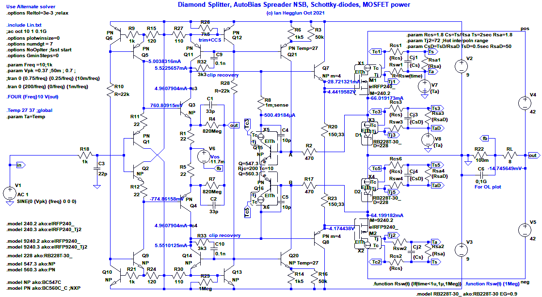
Autobias with Schottky's
This version is similar to the previous one but the MOS-diodes are replaced by Schottky diodes.
Since the Schottky diode temp-co is negative (opposite to MOS-diodes) the Schottky diodes must be thermally linked to the spreaders to prevent thermal runaway.
The circuit below is thermally stable - starting cold at 66mA and ending at 73mA after 50 seconds. The crossover current peaks at 2 seconds at 95mA which is acceptable.
.
Using Schottky's rather than MOS-diodes allows autobias to operate over the full output range down to 60mA (was 250mA) because the dynamic resistance of the diodes is lower than the MOSFETs as diodes. The advantage of MOS-diodes is thermal coupling to the spreaders is not needed.
The Schottky diodes have a thermal resistance (Rsa) of 50C/W which is effectively just a TO-220's on a PCB (no added heatsink). Thermal coupling to the spreaders (Q15, Q16) is Rjc of 200C/W with time constant of 10 seconds which I have used for a TO-92 thermally coupled to a TO-220 Schottky package (a guess until bench tests - such data is hard to get from datasheets). With about 30W output the Schottky's temperature rise above ambient is 15C, while the main heatsink used here rises by 40C above ambient. So the Schottky's should run cool even without their own heatsink. But mounting the Schottky's on the main heatsink seems to be detrimental. You can check this by editing "Tc3" (in 2 places) and "Tc5" (2 places) to "Tc".
There's a lot more that I could explain about the electrothermal subcircuits but that is best covered in another thread. For now feel free to ask questions in this thread. One thing is the ".param Tj2=72 ;Hot interpoln range" card. I have had trouble with LT-XVII when Tj2 is set above 80C (it wont start). But this setting is not an issue with LT-IV which I use. This parameter sets the valid interpolation range for the subcircuit and should be set to the highest likely junction temperature during the run.
The sim still works in LT-XVII if the junction temperature exceeds this value but then it is extrapolation which is becomes less accurate (but still useful).
Since Mike Engelhardt is no loner actively fixing problems with LTspice I'm not expecting this issue to be fixed. So if you need a high Tj simulation (above 150C) then use LT-IV. And if you want the latest model updates in LT-IV then copy the latest LT-XVII libraries across.
Attachments
Bug fix and Update
Hi All,
For the previous electrothermal simulations I found a problem with switching a resistor from 1u ohm to 1Meg. Probably not a bug but a dynamic range issue (even with double precision and the Alternate solver). Changing the switch to 1m ohms and 1 Meg allows it to find the operating point in most cases and is faster starting.
The resistor switch is used to clamp the RC thermal model to ambient to disable the electrothermal feedback so the operating point can be found, then the transient simulation can start and after 1us the switch opens and the electrothermal feedback become active. You can select an alternate switch that is stuck on 1Meg so you can start at the warmed up idle temperature. But sometimes LTspice can't start because it can't find the warmed up operating point. (If that fails you can find the warmed up operating point by starting cold and doing a run with no input signal).
I also found a bug in my electrothermal MOSFET subcircuit for the gate voltage temperature coefficient - it is now referenced to the MOSFETs 'Tnom' value (usually 25C from datasheet plots). The attached electrothermal files have the updated subcircuits - delete or over-write any earlier ones you may have downloaded.
Attached are the updated electrothermal files for the previous Schottky diode autobias method.
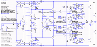
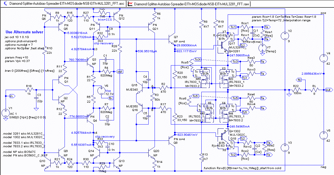
Also attached are the electrothermal files for the MOS-diode method with autobias. Circuit below shows the electrothermal sim for BJT power transistors (Q17, Q18) and MOS-diodes for autobias.
.
The idle current from cold is 250mA and during heating at high output power the crossover current stays within about 10mA of this. Also changing Q17, Q18 to MOSFETs without changing any idle current settings (apart from the Locanthi resistor), the idle current is 220mA. Proof the Autobias loop operates as expected. Notice it does not use emitter/source resistors - the MOS-diodes eliminate them and they do not get hot, even without a heatsink.
Using MOS-diodes rather than Schottky's makes the idle/crossover very temperature stable. One thing not yet determined are the time constants when the MOSFETs are thermally coupled. The time constants I used are deliberately shrunk so the simulation does not take weeks to reach steady state (like 99% of the final values). I shrunk the heatsink time constant from about 2000 seconds to 2 seconds and the MOS-diodes to 0.1s so steady state can be reached in 20 seconds real-time, which takes around 5 minutes on my PC.
This completes the initial phase of this thread - a wideband non-switching autobias power amplifier that is thermally stable without emitter/source resistors, and robust, and not too complex. It clips cleanly and gracefully handles any RF input at full power without cross-conduction issues. It can use power MOSFETs or BJT's interchangeably.
Sounds too good to be true. Anyone want to try it? This idea is open source - (only my schematics have copyright). If you prefer, PM me.
Cheers,
IanHegglun
Hi All,
For the previous electrothermal simulations I found a problem with switching a resistor from 1u ohm to 1Meg. Probably not a bug but a dynamic range issue (even with double precision and the Alternate solver). Changing the switch to 1m ohms and 1 Meg allows it to find the operating point in most cases and is faster starting.
The resistor switch is used to clamp the RC thermal model to ambient to disable the electrothermal feedback so the operating point can be found, then the transient simulation can start and after 1us the switch opens and the electrothermal feedback become active. You can select an alternate switch that is stuck on 1Meg so you can start at the warmed up idle temperature. But sometimes LTspice can't start because it can't find the warmed up operating point. (If that fails you can find the warmed up operating point by starting cold and doing a run with no input signal).
I also found a bug in my electrothermal MOSFET subcircuit for the gate voltage temperature coefficient - it is now referenced to the MOSFETs 'Tnom' value (usually 25C from datasheet plots). The attached electrothermal files have the updated subcircuits - delete or over-write any earlier ones you may have downloaded.
Attached are the updated electrothermal files for the previous Schottky diode autobias method.
Also attached are the electrothermal files for the MOS-diode method with autobias. Circuit below shows the electrothermal sim for BJT power transistors (Q17, Q18) and MOS-diodes for autobias.
.
The idle current from cold is 250mA and during heating at high output power the crossover current stays within about 10mA of this. Also changing Q17, Q18 to MOSFETs without changing any idle current settings (apart from the Locanthi resistor), the idle current is 220mA. Proof the Autobias loop operates as expected. Notice it does not use emitter/source resistors - the MOS-diodes eliminate them and they do not get hot, even without a heatsink.
Using MOS-diodes rather than Schottky's makes the idle/crossover very temperature stable. One thing not yet determined are the time constants when the MOSFETs are thermally coupled. The time constants I used are deliberately shrunk so the simulation does not take weeks to reach steady state (like 99% of the final values). I shrunk the heatsink time constant from about 2000 seconds to 2 seconds and the MOS-diodes to 0.1s so steady state can be reached in 20 seconds real-time, which takes around 5 minutes on my PC.
This completes the initial phase of this thread - a wideband non-switching autobias power amplifier that is thermally stable without emitter/source resistors, and robust, and not too complex. It clips cleanly and gracefully handles any RF input at full power without cross-conduction issues. It can use power MOSFETs or BJT's interchangeably.
Sounds too good to be true. Anyone want to try it? This idea is open source - (only my schematics have copyright). If you prefer, PM me.
Cheers,
IanHegglun
Attachments
-
 Diamond-Splitter-Autobias-Spreader-ElTh-MOSdiode-NSB-ElTh-MJL3281-cct.png56.3 KB · Views: 1,176
 -
Diamond-Splitter-Autobias-Spreader-MOSdiode-NSB-ElTh.zip30.4 KB · Views: 169
-
Diamond-Splitter-Autobias-Spreader-MOSdiode-NSB.zip19.6 KB · Views: 149
-
Diamond-Splitter-Autobias-Spreader-Schottky-NSB.zip38.8 KB · Views: 132
Hi Ian!
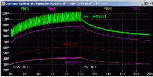
unbelivable!
wingspread is so acurate, hf harmonics at full power are descending so quickly!
unbelivable!
wingspread is so acurate, hf harmonics at full power are descending so quickly!
Attachments
Last edited:
Hello Mr. Hegglun and all,
Thank you again for your gracious past posts in the thread "Class aP amplification"/ Pass Labs Forum.
Does the title of your current thread embody the approach in Class aP amplification?
Best wishes
Anton
Thank you again for your gracious past posts in the thread "Class aP amplification"/ Pass Labs Forum.
Does the title of your current thread embody the approach in Class aP amplification?
Best wishes
Anton
Hi Anton,
Time flies! Our discussions were 2018. For those interested the Blomley thread Post The Blomley Class B amplifier see Posts 24 and 29, and in the Pass-Labs Class-aP thread Post 218.
As I understand your concept you are using a precision rectifier for the splitter function. This was also suggested in the WW Blomley amp article but Peter Blomley used all discretes and no opamps IC's. In those days opamps used lateral PNP transistors which we too slow for precision audio but modern opamps using the latest 30GHz PNP transistors can be used for your approach in audio amps.
Your approach is not be the only way to lower crossover distortion. The opamp with feedback around the whole amp will reduce all the other distortions as well as crossover distortion. EG see Post 20 and Post 59 where THD at 1kHz can be well below 1ppm (Caveat: in a sim!)
Your question about my "diamond splitter" approach. It does not use the precision rectifier approach. It uses global feedback to the splitters to correct for distortion created in the splitters just like most CFA's (with slight variations see Post 63). There is still the annoying input offset voltage problem of CFA's due to slightly different PNP/NPN physics. I am happy to use a trimpot for that.
The main feature of my final version with MOS-diodes is autobias which is fast and thermally robust without source/emitter resistors and easy to compensate at HF. And to boot it gives non-switching currents. Like any idea, don't be surprised if it has been tried before. Or has it?
My example circuits uses voltage gain in the output stage with a +/-9 volt floating supply. I prefer this as it allows low voltage low power transistors. Also current sensing makes it a transconductance amp - I prefer this as it reduces speaker distortion. It is easy to change a the feedback resistors to make it voltage drive.
Overall, designing audio power amps that don't blow up with RF is not that easy. The easy part seems to be getting the distortion low enough. The hard part is 1) to get it to recover from clipping cleanly, and 2) avoid cross-conduction when the input is fed with high levels of RF which seems to overheat most amps, and if left long enough, blow up. The autobias circuit I use here seems (from sims) to be robust against RF. I also saw this in sims of the LT1166 in Post 27 when driving the Vin pin.
Coincidentally, my circuit is similar to driving the Vin pin of the LT1166. But my autobias loop is faster than the LT1166 even when using slower discretes. (I think the LT1166 transistors in the LTspice model are 2-3GHz - does anyone know what is used in manufacture?)
Cheers,
IanH
Hi Ian,
Thanks for your reply and your gracious content of information therein and in this thread too. I need to go back to post #1 and learn your achievements. Your approach is new and interesting to me. It is an intensive course of amp design to study and unravel.
Best wishes
Anton
Thanks for your reply and your gracious content of information therein and in this thread too. I need to go back to post #1 and learn your achievements. Your approach is new and interesting to me. It is an intensive course of amp design to study and unravel.
Best wishes
Anton
IGBT version
Hi All,
Here is an attempt at using IGBTs in place of power MOSFETs or BJTs.
.
Files are attached including the ElectroThermal version. The demo files to plot my IGBT models against the LTspice IGBT internal model. (A white paper on how they work and how the ElectroThermal subcircuits work and how to use them is not ready just yet.) The subcircuits have been updated yet again so I also include the updated earlier amp files.
The IGBT I chose to model is based on the GT50J101 LTspice Ritchie IGBT model (see 'Z' in the help file) and made a symmetrical P-version. It is a fast IGBT but I haven't checked if compensation needs tweaking or cross-conduction with RF signals. So far IGBTs looks feasible.
I noticed 1MHz IGBTs are now available in P and N, eg, OnSemi FGH75T65SHDTL4 p-IGBT 200A 650V 1MHz 76ns 126nC TO-247 at a nice price. An n-IGBT like the FGAF40N60SMD might work OK in this amp with this pIGBT. There are lots more N's to choose from to match to this p-IGBT. I can make a few more IGBT models of available IGBTs if anyone is interested.
As for biasing - I just dropped my IGBT models in place of IRFP240's and the bias was about the same without changing the Autobias settings. As mentioned earlier you can drop in MJL3281's and MJL1302's (or whatever) in place of MOSFETs or IGBTs and get about the same bias current. And THD doesn't change much no matter what power devices are used. All sims so far, no bench trials yet.
Attachments
-
 Diamond-Splitter-Autobias-Spreader-MOSdiode-NSB-IGBT-cct.png19.8 KB · Views: 945
 -
Diamond-Splitter-Autobias-Spreader-MOSdiode-NSB-IGBT.zip11.9 KB · Views: 157
-
Diamond-Splitter-Autobias-Spreader-ElTh-MOSdiode-NSB-ElTh-IGBT.zip23.5 KB · Views: 137
-
Diamond-Splitter-Autobias-Spreader-ElTh-MOSdiode-NSB-ElTh-NewMQ.zip31.3 KB · Views: 167
-
MQZ-demos.zip29.2 KB · Views: 149
Ian, the idea of using trench mos seems like the magic bullet. With irfz44 mosdiode I'm getting ppm level thd @ 1W complementary mosfet output @ 650ma in my sim, except for the usual Vgsth variance that could easily turn into a production nightmare. Do you have any practical suggestion on how to deal with it?
- Home
- Amplifiers
- Solid State
- Towards a wideband non switching Auto Bias power amp