Syn08 (Ovidiu) said this about implementing an Auto Bias loop here:
Well, there's the challenge. A wideband non switching Auto Bias amplifier circuit that works, doesn't oscillate and blow up, and is not too complex.
And if anyone has built a successful amplifier using an auto bias circuit then we'd love to hear how you did it, etc.
Cheers,
Ian
Yeah, did that years ago. Interestingly the output stage used your D2S idea from EW+WW Sep 95. Output devices were 2SJ162/2SK1058 and I used an op-amp for DC servo. It measured flat to 80 kHz according to Silicon Chip magazine and supplied 35 watts with no global NFB and no caps in the signal path.
Nice little amp. I still have the protoypes around somewhere.
Edit: Now that I think about it, there was a need to twiddle trimmers to set the Iq in the output devices, so it wasn't entirely auto-bias. Given consistent devices a fixed resistor would suffice, but that's asking a lot.
Last edited:
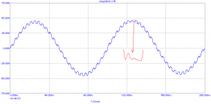
Stability test
As a matter of fact, my simulations did reveal a stability issue. See the picture below, which shows a so called 'R.C. Bowes stability test', where a small 250kHz square wave is superimposed on a large 10kHz sine wave. Clearly some ringing is visible. Enough reason to ring the alarm bell.
But you and me have underestimated (or even ignored) the impact of this ringing.
tried?[...]
This approach is obviously inferior to the geometric collector/drain currents approach used by the LT1166 and that Edmond tried to simulate (which I believe is the best strategy) - unfortunately I still have to see an implementation that works properly.
As a matter of fact, my simulations did reveal a stability issue. See the picture below, which shows a so called 'R.C. Bowes stability test', where a small 250kHz square wave is superimposed on a large 10kHz sine wave. Clearly some ringing is visible. Enough reason to ring the alarm bell.
But you and me have underestimated (or even ignored) the impact of this ringing.
Attachments
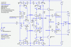
A relative of the last post with a normal voltage opamp by using an output stage with voltage gain.
THD is higher (1W 0.3ppm) and overall BW is higher (8 MHz).
Although this and last post are not Auto Bias they allow a comparison to a conventional bias sensor -- to help decide whether an Auto Bias scheme is worth the extra effort.
Here's another output stage with voltage gain -- but no opamp and a diamond spreader-splitter (so no 10mF base capacitors).
Effectively this is a CFA with voltage gain. One difference is the input transistors (Q1,Q2) are operated at a similar current (5mA) to the spreader-splitter) transistors (Q3,Q4). The idea is the upper transistor's (Q1,Q3) Vbe's match the lower transistor's (Q2,Q4) Vbe's to minimise the output offset voltage (YTB confirmed on the bench).
The feedback is also slightly different with two feedback resistors (R4,R7 matched to 0.1%). This gives slightly better loop gain and hence more feedback. The loop gain with R22 shorted is about 83dB. R22 provides some local degeneration. C1 and C2 provide compensation and C3 is needed when the input is open. C3 can be increased to act as the input filter (eg 800kHz with 100pF and 250kHz 330pF). The slew rate is sufficient for full swing to 250kHz (80V/us).
A SMD thermistor is mounted on the MOSFET leg for a faster bias response time (see peufeu here) so TLD becomes a non issue. (This arrangement is tentative and still needs bench testing).
This is a good circuit to compare to auto bias amps to since THD and BW are better than ordinary (0.4 ppm at 1W 1kHz, 8MHz BW). It is CD/DAC source ready.
For those not familiar with floating supplies you can get two channels form a dual secondary transformer using a pseudo centre tap (two rail caps with 1k balancing resistors) and this give speaker protection from dc (if a MOSFET fails as a short).
BTW it uses low voltage BJT's including low cost, fast, high gain, high Early SMD/TO-92 drivers. To parallel 4 the SMD/TO-92 drivers use individual emitter R's (4x1k2) and individual gate R's (8x47R). The 9V supply is chosen to get enough current into 4 ohms plus a small margin. The Schottky diodes are for antisaturation for faster recovery from clipping.
Attachments
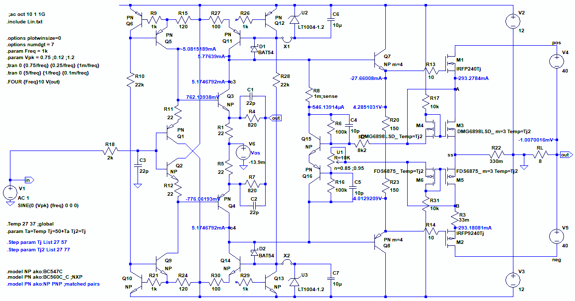
Checking temperature compensation by simulation
The circuit has been modified (below) and checked for output offset voltage with mismatched PNP to NPN's.
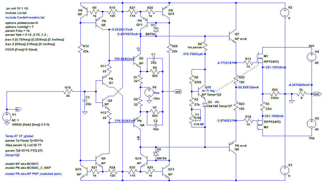
NPN's are assigned as "NP" using .model NP ako:BC5xx. Likewise the PNP's using .model PN ako:BC5xx. So they are now easy to change. I found the BC550C and BC560C Philips models in the Brododynov file collection but they had low VAF values (Early effect), the 'BC560C_C' by NXP was the best. There was no BC550C by NXP so I had to find a NPN match that gave the smallest output offset voltage; I found the BC547C was lowest with -450mV. I added V6 to the emitters of the splitters Q3,Q4 to trim the remaining output voltage. It looks like the PNP-NPN cancellation won't work as hoped, at least for the output offset voltage, so an offset trimpot is needed. But the circuit does cancel ambient temperature changes😎
Another mod: MOSFET thermal compensation now uses a standard type Vbe multiplier rather than a thermistor. It is probably safer in preventing inadvertent disastrous idle currents, and it's easier to get to work than getting the right thermistor and resistor combinations.
With Q15 is sensing the MOSFETs drain lead a diode is needed in the emitter of Q15 to get the right temp co. Stepping ambient temperature shows the diode drop should not change with ambient (a thermistor at ambient will be added to compensate for this). Still, bench tests are needed to check these sims. If instead Q15 is mounted on the heatsink then the diode is not needed (change the Tj2 equation attenuation factor of '0.7' to '0.5' or '0.4'). But the time lag is then minutes instead of seconds.
Other minor changes are source degeneration is now 330mR, C1,C2,C3 all 22pF to give a clean clip recovery. BW is now 3MHz and THD about the same.
Now with a Vbe multiplier the circuit looks a lot like the conventional CFA --except it uses all small LV BJT's and has voltage gain.
The +/-9V supply can be supplied using a 2W DCDC converter from the floating supply and one converter can supply 2 channels.
I'll look at options for paralleling the MOSFETs without current sharing resistors later.
The idea is the upper transistor's (Q1,Q3) Vbe's match the lower transistor's (Q2,Q4) Vbe's to minimise the output offset voltage...
The circuit has been modified (below) and checked for output offset voltage with mismatched PNP to NPN's.
NPN's are assigned as "NP" using .model NP ako:BC5xx. Likewise the PNP's using .model PN ako:BC5xx. So they are now easy to change. I found the BC550C and BC560C Philips models in the Brododynov file collection but they had low VAF values (Early effect), the 'BC560C_C' by NXP was the best. There was no BC550C by NXP so I had to find a NPN match that gave the smallest output offset voltage; I found the BC547C was lowest with -450mV. I added V6 to the emitters of the splitters Q3,Q4 to trim the remaining output voltage. It looks like the PNP-NPN cancellation won't work as hoped, at least for the output offset voltage, so an offset trimpot is needed. But the circuit does cancel ambient temperature changes😎
Another mod: MOSFET thermal compensation now uses a standard type Vbe multiplier rather than a thermistor. It is probably safer in preventing inadvertent disastrous idle currents, and it's easier to get to work than getting the right thermistor and resistor combinations.
With Q15 is sensing the MOSFETs drain lead a diode is needed in the emitter of Q15 to get the right temp co. Stepping ambient temperature shows the diode drop should not change with ambient (a thermistor at ambient will be added to compensate for this). Still, bench tests are needed to check these sims. If instead Q15 is mounted on the heatsink then the diode is not needed (change the Tj2 equation attenuation factor of '0.7' to '0.5' or '0.4'). But the time lag is then minutes instead of seconds.
Other minor changes are source degeneration is now 330mR, C1,C2,C3 all 22pF to give a clean clip recovery. BW is now 3MHz and THD about the same.
Now with a Vbe multiplier the circuit looks a lot like the conventional CFA --except it uses all small LV BJT's and has voltage gain.
The +/-9V supply can be supplied using a 2W DCDC converter from the floating supply and one converter can supply 2 channels.
I'll look at options for paralleling the MOSFETs without current sharing resistors later.
Attachments
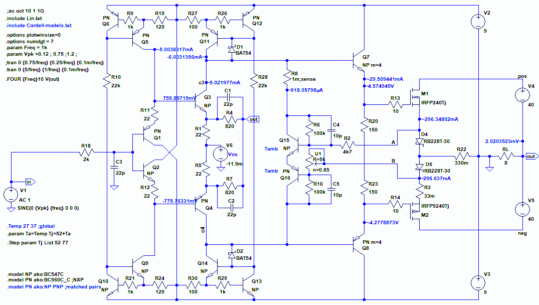
Adding a NSB loop using Schottky diodes
Adding non-switching using Schottky diodes in place of source resistors as peufeu here Power amp OUTPUT STAGE measurements shootout as per 1984 patent NL8403265A - Push=pull transistor power amplifier - has group of three resistors enabling pseudo class=A operation with quiescent current of class=AB type
- Google Patents by E Van Drecht.
.
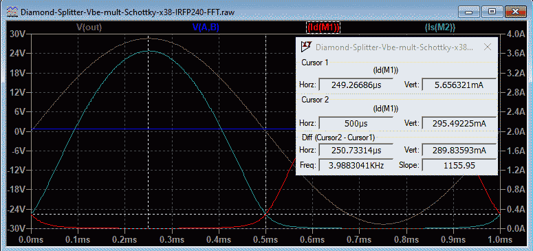
The Schottky diodes are 15A 30V with a low series resistance and dissipate about 0.5W each. The Rush Vbe multiplier senses the total voltage for the two Schottky diodes of about 0.7V. A trimpot is used for trimming the idle current to 300mA for minimum THD at full output, giving about 0.004% at 1kHz. The "off" current is about 5mA (below)
.
Although non-switching is not much use for MOSFETs, this arrangement does give some common mode current sensing feedback which stops the idle current from increasing with temperature, both the MOSFET junction temperature and ambient temperature .
.
It means the Vbe multiplier can be at ambient temperature -- yes, no need to link it to the MOSFET or heatsink😎. So it is like an auto-bias loop that is insensitive to the MOSFETs junction temperature, except here the bias trimpot is still required. That's no big deal for DIY. The bias loop appears to be wideband (yet to check) and easy to compensate separately to the main feedback.
Thanks peufu for the idea😉. Looking good.
Adding non-switching using Schottky diodes in place of source resistors as peufeu here Power amp OUTPUT STAGE measurements shootout as per 1984 patent NL8403265A - Push=pull transistor power amplifier - has group of three resistors enabling pseudo class=A operation with quiescent current of class=AB type
- Google Patents by E Van Drecht.
.
The Schottky diodes are 15A 30V with a low series resistance and dissipate about 0.5W each. The Rush Vbe multiplier senses the total voltage for the two Schottky diodes of about 0.7V. A trimpot is used for trimming the idle current to 300mA for minimum THD at full output, giving about 0.004% at 1kHz. The "off" current is about 5mA (below)
.
Although non-switching is not much use for MOSFETs, this arrangement does give some common mode current sensing feedback which stops the idle current from increasing with temperature, both the MOSFET junction temperature and ambient temperature
. It means the Vbe multiplier can be at ambient temperature -- yes, no need to link it to the MOSFET or heatsink😎. So it is like an auto-bias loop that is insensitive to the MOSFETs junction temperature, except here the bias trimpot is still required. That's no big deal for DIY. The bias loop appears to be wideband (yet to check) and easy to compensate separately to the main feedback.
Thanks peufu for the idea😉. Looking good.
Attachments


Since the diodes don't need a heat sink, if you use TO-220 or TO-126 bias transistors you can couple them with the TO-220 diodes, back to back, with just a silpad for isolation between the two. That gives excellent tracking. I did the test but I forgot to post the results.
Hi peufeu,
But did you this?
But did you this?
That includes temp changes in the Schottky diodes. Well, that's if LTspice is right and I haven't messed up the sims😱.It means the Vbe multiplier can be at ambient temperature -- yes, no need to link it to the MOSFET or heatsink
I didn't couple them because the layout of the board didn't suit it.
Without heat sink the diodes do heat up at high current, so their Vf decreases, and that caused some overbias. It didn't run away, but then I only tested up to 2.5A peak output continuously.
For a full power test of a 100W amplifier into 4 ohms, then that's 7A peak. You'd have to run that in spice, get the average dissipated power in the diode, check with RthJ-A and see how much it heats. The bias probably won't run away, but if it increases significantly, it means the amp will cheat on high power THD tests 😀
Oops
Hi peufeu,
You are right, diode heating causes significant increase in bias current. And tight thermal coupling like you said compensates away the diodes temperature increase. So there will be thermal lag. And I thought for a while it was gone. It did sound too good to be true at the time😉
So I have updated my previous sim file (attached). it now includes diode temperature rise and has thermal coupling to the bias spreader.
For my simulation I chose a 20 C/W heatsink for each diode. My amp at 50W output heats each diode with 0.6W average or 12 deg. I set the idle current to 300mA when both are hot. At startup both are at ambient and the idle current is 345mA. Then with hot diodes and a cold sensor (due to warmup delay) the idle current is 500mA😱. But I haven't checked yet if thermal runaway can occur.
Attachments
Last edited:
That's the test with a BYV29-200 diode (labeled "power device" in the plot) and a D44H11 as bias sensor, they're held back to back with a screw and some Keratherm Red silpad in between for isolation. I did it a while ago, so the diode isn't the same Schottky that I used to test for distortion, I ordered those later.
As you can see the tracking is excellent and there is almost no delay, both in heating and cooling. 0.1°C difference at 1W dissipated power, so if your average power is 0.6W, it'll be even lower. Diode temperature jumps a little bit at the beginning, that's its RthJ-C. The sensor follows the temperature of the back of the TO-220 diode quite well, the lag is maybe 0.1s or something, so it isn't significant. Basically, it works. Any TO-220 or TO-129 transistor used as sensor should work just as well.
If you put a heatsink between the two, then that will add some lag due to thermal mass, and the gain of the thermal probe will be lower since the heatsink will absorb some of the heat. So if a heatsink is necessary I would use someting with low thermal mass like a small thin copper sheet sandwiched between the diode and the sensing transistor. It doesn't need to be large since dissipated power is pretty low.
Attachments
Last edited:
Adding non-switching using Schottky diodes...
Dear Ian!
how about paralleling output mosfets for driving 3 Ohms loads? ;-)
Realy great and (rather) simply circuit, kind congratulations!
Wideband non-switching auto bias topology
Here is textbook-type wideband non-switching auto bias circuitry.
1. No guess work. It guarantees to work, in simulation, almost, (if you bias above 300mA or with larger Re).
2. R2 can be replaced with 100 Ohm potentiometer, to make bias adjustable.
Is it worth the efforts?
Probably no, the improvement is less than 10dB THD@10KHz in my simulation. Around 5dB in most case.
Last edited:
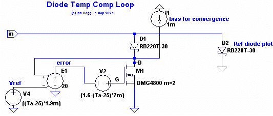
Temp comp for the Schottky's?
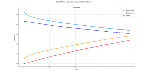
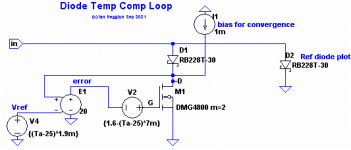
Another way to compensate the Schottky diodes causing bias change is to add a low Ron MOSFET in series with each diode that adds a small voltage to the diodes as they heat up. Since they don't rise more than 25C above ambient the added voltage is only about 30mV. That may not sound much but it can easily double the idle current. The circuit below shows how the Schottky voltage change with temperature can be offset using a feedback loop of Vds. The reference voltage is the case temperature of the Schottky diode, eg, from a Vbe multiplier or IC.

D2 plot shows the effect of changing temperature from 25C to 75C.
D1 plot shows very small difference for the same temperature change.
This D1/MOSFET loop can be used in the amplifier in Post 65 which does not need any other thermal compensation. The thermal tracking accuracy will then be mainly determined by any thermal lag in the diode compensation loop, which can hopefully be made small enough.
The MOSFET chosen is the DMG4800 which is a dual 20mR SO-8. The error amplifier E1 will need to be fast since it senses Vds due to the output stage signal, maybe 1MHz for a wideband design. This is just proof of concept.
Hi peufeu, You are right, diode heating causes significant increase in bias current. And tight thermal coupling like you said compensates away the diodes temperature increase. So there will be thermal lag. And I thought for a while it was gone. It did sound too good to be true at the time😉...
Another way to compensate the Schottky diodes causing bias change is to add a low Ron MOSFET in series with each diode that adds a small voltage to the diodes as they heat up. Since they don't rise more than 25C above ambient the added voltage is only about 30mV. That may not sound much but it can easily double the idle current. The circuit below shows how the Schottky voltage change with temperature can be offset using a feedback loop of Vds. The reference voltage is the case temperature of the Schottky diode, eg, from a Vbe multiplier or IC.
D2 plot shows the effect of changing temperature from 25C to 75C.
D1 plot shows very small difference for the same temperature change.
This D1/MOSFET loop can be used in the amplifier in Post 65 which does not need any other thermal compensation. The thermal tracking accuracy will then be mainly determined by any thermal lag in the diode compensation loop, which can hopefully be made small enough.
The MOSFET chosen is the DMG4800 which is a dual 20mR SO-8. The error amplifier E1 will need to be fast since it senses Vds due to the output stage signal, maybe 1MHz for a wideband design. This is just proof of concept.
Attachments
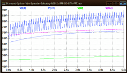
Checking current sharing with an electrothermal simulation
The circuit here uses parallel IRFP240/9240 for 3 ohms.
To check current sharing electrothermal models are used. Normal SPICE models are isothermal which means the temperature of the MOSFETs stays the same during a run. This electrothermal model takes account of the temperatures of the MOSFETs during a run. So we can see in this circuit if currents share (or not) as their temperatures change; if one starts to hog the current when it heats up more than the other.

.
The first plot shows the currents in the two n-MOSFETs as they heat up from idle with a 25V output (100W/3R). This is with two matched n-MOSFET's. Case temperatures Tc1 for M1 and Tc3 for M3 are the same.
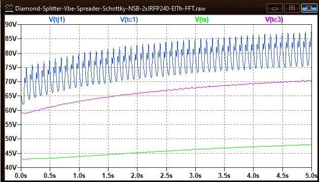
.
Now adding 50mV to the gate of M3, to simulate a threshold voltage mismatch between the two n-MOSFETs, causes its idle current to be about 100mA higher (30% more heating than M1).
.
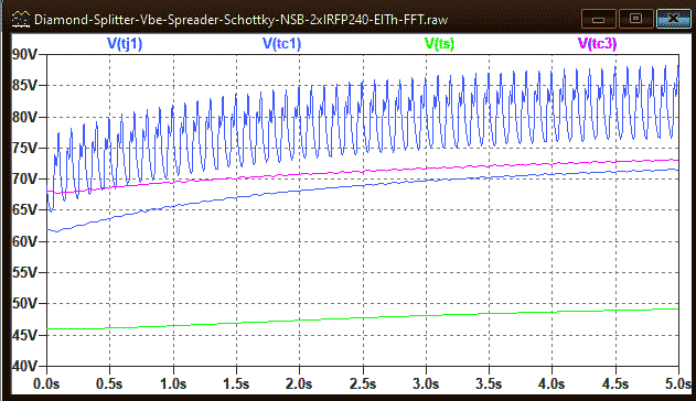
.
This shows the case temperature Tc3 for M3 at the start is about 5 degrees more than Tc1 (read 50V as 50C). But after their temperatures stabilise the case temperatures move closer together which means current hogging does not occur in this circuit.
BTW we can check the final heatsink temperature with 100W output and it reaches about 50 degrees with 27C ambient. The heatsink is Rsa/4 where Rsa=1.8K/W per MOSFET, or 0.45K/W for one channel, typical for a 100W Class-AB amp.
BTW2 this circuit is only checking the MOSFETs bias loop in real time. It does not allow the effect of the Schottky diode heating to be simulated in real time. This is OK since I am assuming the Schottky diodes temperature rise can be cancelled using the method in the previous post. When this is done the bias loop controls the idle current while the MOSFET's are heating up and there is no need for thermal coupling of the spreader transistors to the heatsink. So there will be virtually no thermal delay in the biasing loop (assuming the Schottky diodes thermal loop can be made to operate fast).
Hi Pawel,Dear Ian!
how about paralleling output mosfets for driving 3 Ohms loads? ;-)
Realy great and (rather) simply circuit, kind congratulations!
The circuit here uses parallel IRFP240/9240 for 3 ohms.
To check current sharing electrothermal models are used. Normal SPICE models are isothermal which means the temperature of the MOSFETs stays the same during a run. This electrothermal model takes account of the temperatures of the MOSFETs during a run. So we can see in this circuit if currents share (or not) as their temperatures change; if one starts to hog the current when it heats up more than the other.
.
The first plot shows the currents in the two n-MOSFETs as they heat up from idle with a 25V output (100W/3R). This is with two matched n-MOSFET's. Case temperatures Tc1 for M1 and Tc3 for M3 are the same.
.
Now adding 50mV to the gate of M3, to simulate a threshold voltage mismatch between the two n-MOSFETs, causes its idle current to be about 100mA higher (30% more heating than M1).
.
.
This shows the case temperature Tc3 for M3 at the start is about 5 degrees more than Tc1 (read 50V as 50C). But after their temperatures stabilise the case temperatures move closer together which means current hogging does not occur in this circuit.
BTW we can check the final heatsink temperature with 100W output and it reaches about 50 degrees with 27C ambient. The heatsink is Rsa/4 where Rsa=1.8K/W per MOSFET, or 0.45K/W for one channel, typical for a 100W Class-AB amp.
BTW2 this circuit is only checking the MOSFETs bias loop in real time. It does not allow the effect of the Schottky diode heating to be simulated in real time. This is OK since I am assuming the Schottky diodes temperature rise can be cancelled using the method in the previous post. When this is done the bias loop controls the idle current while the MOSFET's are heating up and there is no need for thermal coupling of the spreader transistors to the heatsink. So there will be virtually no thermal delay in the biasing loop (assuming the Schottky diodes thermal loop can be made to operate fast).
Attachments
-
 Diamond-Splitter-Vbe-Spreader-Schottky-NSB-2xIRFP240-ElTh-Tplots.png9.3 KB · Views: 1,290
 -
 Diamond-Splitter-Vbe-Spreader-Schottky-NSB-2xIRFP240-ElTh-cct.png29.9 KB · Views: 1,323
 -
 Diamond-Splitter-Vbe-Spreader-Schottky-NSB-2xIRFP240-ElTh-Tplot1.png8.9 KB · Views: 1,283
 -
Diamond-Splitter-Vbe-Spreader-Schottky-NSB-2xIRFP240-ElTh-FFT.zip8.8 KB · Views: 162
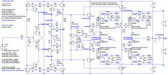
Trench MOSFETs in place of Schottky's
Hi peufeu, All,
Trench MOSFETs can be used in place of Schottky's for Class-AB bias feedback.
.
.
I use SO-8 dual MOSFET's so their threshold voltage variation with temperature is fast tracking. I chose two dual MOSFETs in parallel -- M3 is a pair of dual-FET's in parallel (3 in parallel and one for threshold voltage). Paralleling is to get lower voltage drop and spread the heat over several packages. Likewise for M5. As shown with 3 in parallel the voltage drop is 0.5V at 5A (or 2W peak). That's about the same as a 15A Schottky diode.
I don't have data on thermal linkage between dual MOSFET's for these SO-8 types. Pulse bench tests are needed. There are also Power PAK SO-8 dual devices, but again, no data on their inter-chip thermal linkage.
Apart from some thermal time lag (from diode-MOSFET to the bias-MOSFET) the idle currents in steady state are kept constant in this simulation when temperature stepping any of the following: Tj (power MOSFETs), Tj2 (MOS diodes), and Ta (all globally).
Adding the LT1004's to the current sources (Q11,Q14) keeps the idle current constant with global temperature. The original current sources idle current falls with increasing ambient temperature. If you prefer the original then, reconnect R26 and R29 and opening the links to the LT1004's and change the bias to pot to 0.95 for a similar bias current. A bench version is needed to see if the temperature co's obtained here are realistic.
This looks like a candidate for a low distortion, wideband, (almost) auto bias amplifier. There is still the trimpot for idle current but that is not a major issue for DIY, it may be a feature. There is still some thermal lag (MOS diodes only, not the main MOSFETs), but hopefully it is fast enough to be irrelevant.
Cheers,
Ian
Attachments
Does the "MOSFET as diodes" schematic give the same gm as a standard MOSFET output stage?
Thermal linkage will most likely be quite poor as the two dies are only linked with plastic, they are isolated from each other so they will not have the same leadframe. I would expect a pair of TO-220 FETs screwed together back to back with silpad to track much faster, like the transistor with the TO-220 diode.
I think you could emulate this construction with SMDs, on a 4 layer board. Layer2 is 0.2mm below TopLayer, so if you use SMD MOSFETs with thermal tab (PowerPAK and the like) and not pins like SO-8, then in you could use vias under the tab of one FET to dump heat into a copper pour on Layer2, which would then transfer this heat to a small copper pour on Layer1 on which the other FET's drain tab is soldered. I think this could work, but 0.2mm of prepreg has much higher thermal resistance than a proper silpad, so it probably won't beat the back-to-back TO-220s.
I did measure a SOT-23 DMMT3904 dual matched transistor ; I had one transistor dissipate some power while measuring the other's Vbe at 1mA constant. As you can see, it takes a while for the heat for the first transistor to reach the second one. That makes sense because the dies are side by side so heat has to travel laterally through a small cross section of plastic, which is much worse than through the metal back of a TO-220. Quite a lot of heat goes through the pins so the second transistor only tracks a small portion of the first one's temperature change. I think a dual FET would show similar results.
This also shows that while these dual transistors are nice because they are cheap and matched, they are also not monolithic because they're not a special fabrication, they just pick two adjacent dies on the wafer so they will get a good match, and put the dies on a package. So it's a derivative from an ultra mass produced BJT die, which means no special snowflake low volume expensive monolithic die. But they're not on the same piece of silicon, and the two dies are on different leadframes, so they should have a low delta-T due to external temperature variations which is nice, but if they dissipate some "significant" power (which for a SOT23 is really not much) the thermal tracking goes byebye.
I don't have data on thermal linkage between dual MOSFET's for these SO-8 types. Pulse bench tests are needed. There are also Power PAK SO-8 dual devices, but again, no data on their inter-chip thermal linkage.
Thermal linkage will most likely be quite poor as the two dies are only linked with plastic, they are isolated from each other so they will not have the same leadframe. I would expect a pair of TO-220 FETs screwed together back to back with silpad to track much faster, like the transistor with the TO-220 diode.
I think you could emulate this construction with SMDs, on a 4 layer board. Layer2 is 0.2mm below TopLayer, so if you use SMD MOSFETs with thermal tab (PowerPAK and the like) and not pins like SO-8, then in you could use vias under the tab of one FET to dump heat into a copper pour on Layer2, which would then transfer this heat to a small copper pour on Layer1 on which the other FET's drain tab is soldered. I think this could work, but 0.2mm of prepreg has much higher thermal resistance than a proper silpad, so it probably won't beat the back-to-back TO-220s.
I did measure a SOT-23 DMMT3904 dual matched transistor ; I had one transistor dissipate some power while measuring the other's Vbe at 1mA constant. As you can see, it takes a while for the heat for the first transistor to reach the second one. That makes sense because the dies are side by side so heat has to travel laterally through a small cross section of plastic, which is much worse than through the metal back of a TO-220. Quite a lot of heat goes through the pins so the second transistor only tracks a small portion of the first one's temperature change. I think a dual FET would show similar results.
This also shows that while these dual transistors are nice because they are cheap and matched, they are also not monolithic because they're not a special fabrication, they just pick two adjacent dies on the wafer so they will get a good match, and put the dies on a package. So it's a derivative from an ultra mass produced BJT die, which means no special snowflake low volume expensive monolithic die. But they're not on the same piece of silicon, and the two dies are on different leadframes, so they should have a low delta-T due to external temperature variations which is nice, but if they dissipate some "significant" power (which for a SOT23 is really not much) the thermal tracking goes byebye.
Attachments
Last edited:
Hi peufeu,
Thanks for you ideas.
.
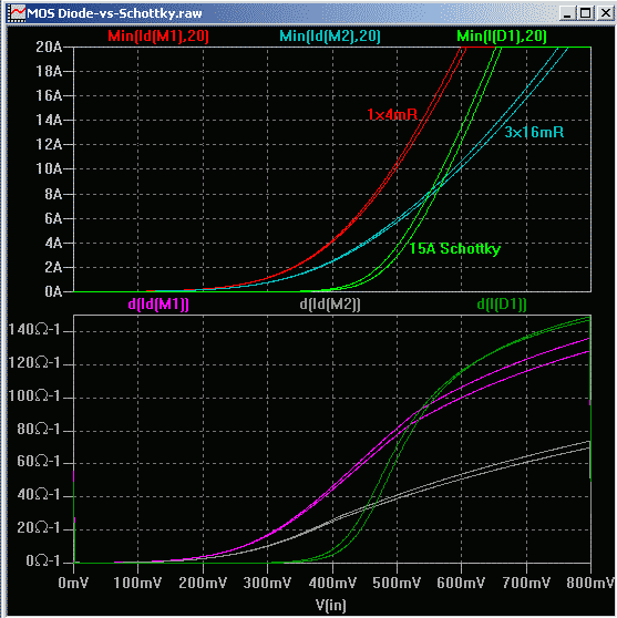
Temperature is stepped 27C and 37C. The Schottky has a positive temp co while the MOS-diodes have a negative temp co.
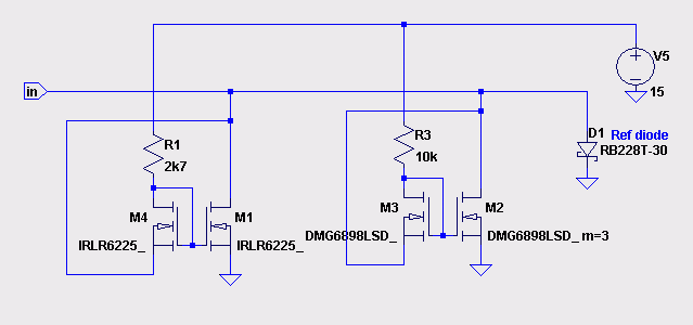
The IRLR6225 is a TO-252 with 4m ohm ON resistance. The DMG6898 are 16m ohms each with 3 in parallel (as per my last amp post).
Thanks for your thoughts on the SO-8 with poor/slow thermal response. So I checked out a TO-252 device. A TO-252 has less copper than a TO-220 and can change temperature faster - so two can be coupled back-back with an insulating pad. If the response time is 1-3 seconds then I'd consider that acceptable with my amp.
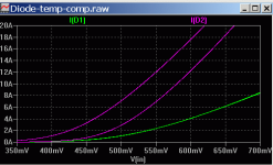
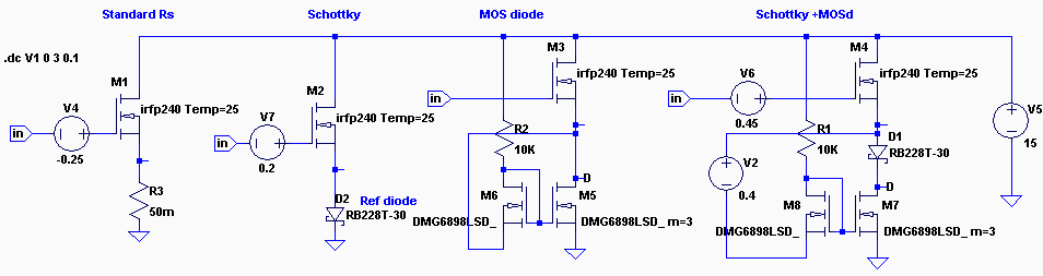
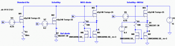
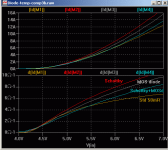
Back to your query. I placed my MOS-diode and a Schottky and a fixed source resistor in a follower test jig to compare Gm plots:
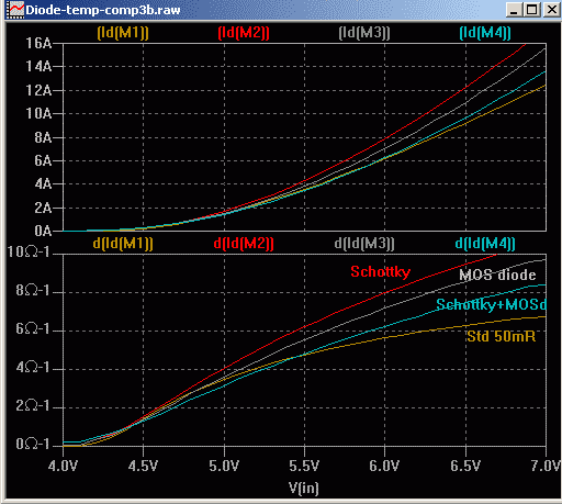
.
The starting voltages were trimmed for about the same voltage. The standard follower has a 50mR source resistor.
The MOS-diode has slightly less Gm than the Schottky. But the MOS-diode has more Gm than the standard follower even with a 50mR source resistor.
The advantage of the MOS-diode over the Schottky as source "resistors" is a slight negative temp-co over our usual current range for the IRFP240 for amplifiers.
The advantages of Schottky's (or MOS-diode) over standard source resistors in Class-AB output stages is to achieve non-switching biasing, plus the output devices are inside the bias feedback loop so their positive temperature co's are controlled (without source resistors).
Thanks for you ideas.
First a test circuit to compare two MOS-diodes with a 15A Schottky and plots:Does the "MOSFET as diodes" schematic give the same gm as a standard MOSFET output stage?
.
Temperature is stepped 27C and 37C. The Schottky has a positive temp co while the MOS-diodes have a negative temp co.
The IRLR6225 is a TO-252 with 4m ohm ON resistance. The DMG6898 are 16m ohms each with 3 in parallel (as per my last amp post).
Thanks for your thoughts on the SO-8 with poor/slow thermal response. So I checked out a TO-252 device. A TO-252 has less copper than a TO-220 and can change temperature faster - so two can be coupled back-back with an insulating pad. If the response time is 1-3 seconds then I'd consider that acceptable with my amp.
Back to your query. I placed my MOS-diode and a Schottky and a fixed source resistor in a follower test jig to compare Gm plots:
.
The starting voltages were trimmed for about the same voltage. The standard follower has a 50mR source resistor.
Code:
Case	M1(Std) 	M2(Sch) 	M3(MOS-d) 	M4(MOS-d+Sch)
Gm@5A	5.3		6.6 		6.2 			5.7
The advantage of the MOS-diode over the Schottky as source "resistors" is a slight negative temp-co over our usual current range for the IRFP240 for amplifiers.
The advantages of Schottky's (or MOS-diode) over standard source resistors in Class-AB output stages is to achieve non-switching biasing, plus the output devices are inside the bias feedback loop so their positive temperature co's are controlled (without source resistors).
Attachments
-
MOS-Diode-vs-Schottky.zip2 KB · Views: 136
-
 MOS Diode-vs-Schottky.png11.5 KB · Views: 1,123
 -
 MOS Diode-vs-Schottky-cct.png3.7 KB · Views: 1,109
 -
 Diode-temp-comp3b-Gm-compare-cct.png5.7 KB · Views: 1,135
 -
 Diode-temp-comp3b-Gm-compare.png8.5 KB · Views: 1,113
 -
Diode-temp-comp3b.zip2.6 KB · Views: 118
Last edited:
Non-complementary MOS-diodes
Here's the amp with IRLR6225's as the MOS-diodes. The IRLR6225 is a TO-252 20V n-channel trench MOSFET with 4m ohm ON resistance. It was featured in the previous post.
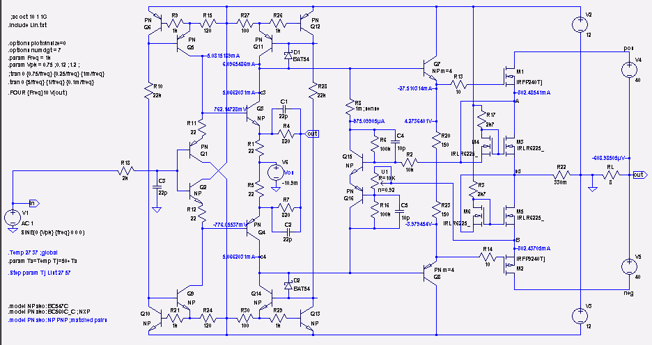
Since the MOS-diode is a two terminal device it does not need a complement for the main p-channel MOSFET (M2).
That is convenient because a good p-channel complements for the likes of the IRLR6225 may be hard to find and anything close will be quite expensive compared to the n-channel.
Power dissipated in the MOS-diodes (M3 and M5) are 0.5W each for 50W output, and 50mW at 1W output and at idle.
Here's the amp with IRLR6225's as the MOS-diodes. The IRLR6225 is a TO-252 20V n-channel trench MOSFET with 4m ohm ON resistance. It was featured in the previous post.
Since the MOS-diode is a two terminal device it does not need a complement for the main p-channel MOSFET (M2).
That is convenient because a good p-channel complements for the likes of the IRLR6225 may be hard to find and anything close will be quite expensive compared to the n-channel.
Power dissipated in the MOS-diodes (M3 and M5) are 0.5W each for 50W output, and 50mW at 1W output and at idle.
Attachments

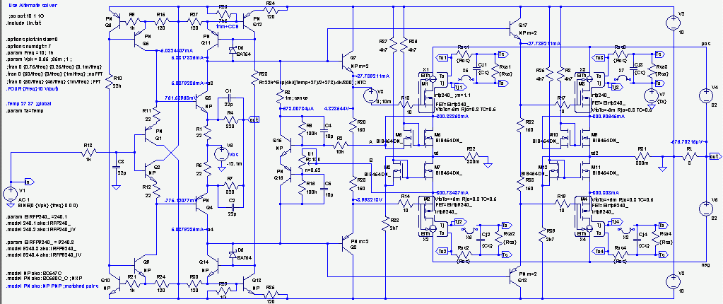
3 ohm 100W version with MOS-diodes + thermistor temp comp for ambient change
HI Pawel,
Here is the 3 ohm 100W version with MOS-diodes and thermistor temperature compensation for ambient changes. It is an update of Post 75 electrothermal simulation with parallel MOSFETs.
.
.
The thermistor temperature compensation corrects for over-temp compensation of the CCS's. Without the this the idle current falls from normal 300mA per pair to 220mA per pair when the ambient temperature changes by 10 degrees.
A 22k NTC thermistor (R22) senses the ambient temperature and changes the voltage on the emitter resistors of Q12 and Q13. The value of the emitter resistors determines the temp-co of Q12 and Q13 CCS. This should work OK for ambient temperatures from +10C to 40C.
This method is better than using the LT1004 voltage reference as in Post 76 because it allows feedback of the CCS output current which raises the output resistance allowing low VAS transistors for Q11,Q14.
This simulation has electrothermal feedback in the main MOSFETsIt shows the change in bias over time when changing the output power from normal 1W average to 100W continuous such as in a bench test.
This simulation does not shows electrothermal feedback of the MOSFET diodes - that will need additional subcircuits for the 8 MOSFETs for the MOS-diodes - probably best done without the paralleling for 3 ohms for less clutter of the schematic. It will also require thermal linkage details that I need to estimate some how.
Attachments

Last edited:
- Home
- Amplifiers
- Solid State
- Towards a wideband non switching Auto Bias power amp