
And the 4 Ohm load:
Attachments
-
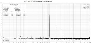 THF-51S DEFISIT Duo Cap 47V 1.74A 4R 1W.jpg184.4 KB · Views: 69
 -
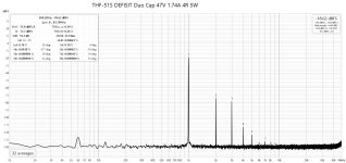 THF-51S DEFISIT Duo Cap 47V 1.74A 4R 5W.jpg184 KB · Views: 68
 -
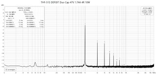 THF-51S DEFISIT Duo Cap 47V 1.74A 4R 10W.jpg184.6 KB · Views: 58
 -
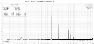 THF-51S DEFISIT Duo Cap 47V 1.74A 4R 20W.jpg184.4 KB · Views: 53
 -
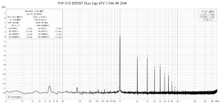 THF-51S DEFISIT Duo Cap 47V 1.74A 4R 25W.jpg185.6 KB · Views: 52
 -
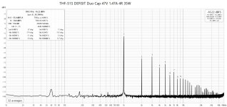 THF-51S DEFISIT Duo Cap 47V 1.74A 4R 35W.jpg187.4 KB · Views: 55
 -
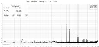 THF-51S DEFISIT Duo Cap 47V 1.74A 4R 30W.jpg186 KB · Views: 54
 -
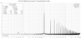 THF-51S DEFISIT Duo Cap 47V 1.74A 4R 36.4W 1% THD.jpg189.3 KB · Views: 60
 -
 THF-51S DEFISIT Duo Cap 47V 1.74A 4R 40W.jpg189.5 KB · Views: 72

Hi Ben, oh please please, you are the "real" man, please do a "Spice" man the favor measure the current in the load and the current in your source resistor and the current in the resistor to the second output cap. (of course the voltages and we can see your resistor values and use Ohm)
I am so eager after my Spice marathon what you can get in real with a 1 Ohm source resistor and the THFs we could buy from Japan concerning MosFet contribution.
Would make me happy!
:--))
I am still waiting for suitable heatsinks.
I am so eager after my Spice marathon what you can get in real with a 1 Ohm source resistor and the THFs we could buy from Japan concerning MosFet contribution.
Would make me happy!
:--))
I am still waiting for suitable heatsinks.
Here are some numbers (resistance values and Vrms measured across the resistance) from my measurement of the as-built right channel, 47VDC power supply and Iq=1.74A:
1. Output load=220R in parallel with 8.2R= 7.9R
Irms=2.49Vrms/7.9R= 0.315A= 315mA, LTSpice Irms=0.707x3.52Vp/8R= 0.311A= 311mA, also Irms=0.707x(439mA+442mA)/2= 311mA
2. Source resistors=5x0.2R=1.0R
Irms=131mVrms/1.0R= 131mV, LTSpice Irms=0.707x(1.935A-1.536A)/2= 141mA
3. Mosfet output resistors=3x0.5R=1.5R
Irms=137mVrms/1.5R= 91mA, LTSpice Irms=(C7 Irms)=0.707x(131mA+137mA)/2= 95mA
4. Mosfet Measured Current = 91mA+131mA= 222mA (output resistor current + source resistors current), LTSpice Mosfet current=0.707x(2.066A-1.401A)/2= 0.235A = 235mA
5. SIT Measured Current = 315mA-222mA= 93mA (Total current - Mosfet current), LTSpice SIT current = 0.707x(1.844A-1.623A)/2= 0.078A = 78mA
6. Mosfet direct to capacitor/Total output at load = 91mA/315mA= 29%, LTSpice =95mA/311mA = 31%
Overall I would say that the LTSpice results were reasonably close to the real life measurements.
*2SK180
*GENERATED BY SIT MODELER @ AUDIOHOBBY.COM
*MODEL RANGE: 100V, 2A
*--------------------------------------------------
.SUBCKT 2SK180 D G S ; Drain Gate Source
+ PARAMS: MU=16 X=1.8 K=0.225 N=1.72 VCT=0 RG=2MEG
*--------------------------------------------------
B1 D S I=K*PWR(URAMP((V(G,S)+VCT)+(N*LN(V(D,S))+(V(D,S)/MU))),X)
FOR MULTISIM COMMENT OUT ABOVE LINE () AND UNCOMMENT NEXT LINE
*B1 D S I=K*PWR(MAX((V(G,S)+VCT)+(N*LN(V(D,S))+(V(D,S)/MU)),0),X)
R1 G S {RG}
CGS G S 1500P
CGD G D 0P
CDS G S 0P
.ENDS 2SK180
*--------------------------------------------------
*--------------------------------------------------
*2SK2087C
*GENERATED BY SIT MODELER @ AUDIOMAKER.TECH
*MODEL RANGE: 20V, 2A
*--------------------------------------------------
.SUBCKT 2SK2087C D G S ; Drain Gate Source
+ PARAMS: MU=100 X=3.53 K=0.376 N=0.69 VCT=0.82 RG=2MEG
*--------------------------------------------------
B1 D S I=K*PWR(URAMP((V(G,S)+VCT)+(N*LN(V(D,S))+(V(D,S)/MU))),X)
R1 G S {RG}
CGS G S 0P
CGD G D 0P
CDS G S 0P
.ENDS 2SK2087C
*--------------------------------------------------
.SUBCKT thf51-1x0063 D G S ; Drain Gate Source
+ PARAMS: MU=43.571 X=1.494 K=1.339 N=0.902 VCT=0.831 RG=5MEG
*--------------------------------------------------
B1 D S I=K*PWR(URAMP((V(G,S)+VCT)+(N*LN(V(D,S))+(V(D,S)/MU))),X)
FOR MULTISIM COMMENT OUT ABOVE LINE () AND UNCOMMENT NEXT LINE
*B1 D S I=K*PWR(MAX((V(G,S)+VCT)+(N*LN(V(D,S))+(V(D,S)/MU)),0),X)
R1 G S {RG}
CGS G S 5000P
CGD G D 5000P
CDS G S 0P
.ENDS thf51-1x0063
.model IXTN40P50PV VDMOS(pchan Vto=-3.0 Kp=7.42 Lambda=2.9m
- Rs=2.2m Rd=0.23 Rds=1e7 Cgdmax=6n Cgdmin=90p a=0.26 Cgs=10nF
- Cjo=8.35nF m=0.68 VJ=2.5 IS=4.0E-06 N=2.4 ksubthres=.22))
Hi Ben, when I calculate in your way the current through the resistor to the second cap divided by the current in the load you have the 29% MosFet contribution, you calculated the same.
When I calculate the contribution in the way Nelson suggested we have (131mV + 91mV) divided by 315mV = 70% Mosfet contribution.
I hope I took all values correct.
So what is the truth.
When I give the way Nelson suggested priority we all must use about 3R between the sources to get the 30%
When I calculate the contribution in the way Nelson suggested we have (131mV + 91mV) divided by 315mV = 70% Mosfet contribution.
I hope I took all values correct.
So what is the truth.
When I give the way Nelson suggested priority we all must use about 3R between the sources to get the 30%
Last edited:
If R11 would be open, would it mean that MOSFET contributed ZERO% current?
I personally think it would not be true.
Could MOSFET contribute some current thru R10?
I personally think it would not be true.
Could MOSFET contribute some current thru R10?
The truth? I don't know what the truth is. 🤓
As for R11, if that is open, simulation showed that the circuit behaved as push-pull, with equal current from SIT and mosfet, with the mosfet current going through R11 and out through C4.
As for R11, if that is open, simulation showed that the circuit behaved as push-pull, with equal current from SIT and mosfet, with the mosfet current going through R11 and out through C4.
I think it is a matter of finding the right combination of resistors. I just tried R10=R11=5R and the results were very promising.
Here are the simulation results:
C4 = 432mA+428mA = 860mAp-p
C7 = 68mAa=70mA = 138mAp-p
R8 = 497mA+499mA = 995mAp-p
U1 source = 2431mA-1708mA = 723mAp-p
M1 source = 2208mA-1933mA = 275mAp-p
U1 source + M1 source = 998mAp-p
(M1 source)/(U1 source + M1 source) = 275/998 = 27.6%

C4 = 432mA+428mA = 860mAp-p
C7 = 68mAa=70mA = 138mAp-p
R8 = 497mA+499mA = 995mAp-p
U1 source = 2431mA-1708mA = 723mAp-p
M1 source = 2208mA-1933mA = 275mAp-p
U1 source + M1 source = 998mAp-p
(M1 source)/(U1 source + M1 source) = 275/998 = 27.6%
The down side of this interpretation is that the 1% THD power at 8R is about 12W.
What is the truth?

What is the truth?
The truth is that you can play with the values of the resistors until you can get at or closer to whatever you desire. If you have perfect ears and taste you can do it without other
equipment. If all you have is a voltmeter and oscillator you can get some objective values,
and with distortion analyzer even more objective results. Maybe one of these will lead you to audio nirvana...
😉
equipment. If all you have is a voltmeter and oscillator you can get some objective values,
and with distortion analyzer even more objective results. Maybe one of these will lead you to audio nirvana...
😉
Nowadays for me even an email from the right person is enough to get to me to audionirvana 🙂)Maybe one of these will lead you to audio nirvana...
Tomorrow! Today nice journey to father Rhine…. To forget all SITs and MosFets. :—))Bruder
Schick me your sim file...... I'm lazy
The one channel that I have built measured well and sounds good, as far as I can tell with only one channel. So my version will stay as is and I will continue on with the other channel.
Here are some more real life test results. I ran some square waves through the amplifier. My old HP 3310A was the source. The amplifier output showed a small amount of high frequency roll-off, but nothing dramatic. The HP wasn't perfect either. The yellow trace was the HP, and the blue trace was the amplifier output. Load was 8 Ohm.
20kHz:
- Home
- Amplifiers
- Pass Labs
- Tokin DEFISIT Duo Capacitor Output Stage Amplifier