- IRS2092 supplies and UVLO:
The 5V regulators can improve signal integrity because the reference for the comparator is derived from the mid point of the rails (and datasheet does not tell anything about implementation), however, the current source effect is not suppressed, there are still "ballast" resistors to the rails, but there is the enable signal already suppressing oscillation. A solution suppressing the oscillation even without an enable signal would be good old zeners buffered with TO-220 (or something mid-power) emitter followers, with no ballast resistors (but this is also the less failure proof topology, something wrong with the followers and the IC would be toasted). I think the pitfall is in IC implementation, the oscillator would probably be avoided if the IC required CSD to go low (before recognizing it high for enable) after each UVLO event.
- Post-filter feedback:
I did some simulation attempts. I was right and wrong at the same time, there are enough elements, but one more pin would be needed in the IC to insert a resistor between OTA output and comparator input. This is because customizing the Q of the HF roll-off to be flat to >20khz requires separating feedback in 2 branches: audio-FB to the input of the integrator and carrier-FB to the input of the comparator. If this is done without the extra pin then the low output impedance of the OTA (wired as non-inv integrator) prevents efficient carrier insertion and does not allow to customize switching frequency. On the other hand, if an external integrator is used then the circuit moves into next "complexity class". The OTA in IRS2092 is wired in such a way that it only allows implementing optimum all-pre-filter feedback (a bit archaic).
- Start-up of gate drive:
VBS means (VB-VS). The -12V switch is not implemented properly, but it is not needed either, the gate drive section obeys both CSD shutdown and (VAA-VSS) UVLO shutdown.
Theoretically, silent turn-on would be achieved by applying enable signal when OTA output is centered (integrator as close as posible to reset) and also centered amplifier output (load and R20 do this bit).
Datasheet mentions something about "COMP pin star-up local oscillation", depending on CSD voltage, "1Mhz" typical, in the classic cryptic IR fashion. There is probably some start-up optimization but only way to understand it is investigating IC behavior in a prototype.
...
If this is done without the extra pin then the low output impedance of the OTA (wired as non-inv integrator) prevents efficient carrier insertion and does not allow to customize switching frequency. On the other hand, if an external integrator is used then the circuit moves into next "complexity class". The OTA in IRS2092 is wired in such a way that it only allows implementing optimum all-pre-filter feedback (a bit archaic).
I also dislike to feed the fast carrier from imput through the entire error correction gain stage. But the OTA is fast enough to do so. Results were better than expected.
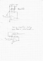
Here the starting point according to the feedback structure „Basic“ of my post with the evolutionary feedback structures. The basic version has only PD structure, not PID.
C_fb has double function. The current in C_fb is forming not just the derivative portion for the PD regulator, but it also forms the basis for triangular carrier for the modulator.
The carrier residuals of the output voltage carry the integral of the triangular HF currents in the choke. The current in C_fb forms the derivative of the output voltage (ic=C* di/dt).
This triangular current from C_fb together with the OTA and R2 then forms the triangular carrier at COMP. Superimposed to this carrier you have the audio signal and error correction signal.
C2 can be helpful for tuning the frequency compensation, but it is even more helpful to customize the switching frequency. For simplicity in the equations below C2 is neglected.
If you want to calculate fs by hand you would need to extend these equations by the equations of C2 and also take the constant delay and output filter into account.
Do we need more? For basic function not – for performance tuning yes.
With this PD structure you cannot surpass the level of UcD.
If you want to become better, you need more loop gain, i.e. by adding one cap to get additional integrating gain. Feel free to simulate the next evolutions and find the structure you like best.
Feel free to step into math, here the equations for starting:
V_COMP(t)= -1*(Vin(t) *R2/R1 + Vout(t)*R2/R_fb + C_fb*dVout(t)/dt)
VS = +35V for V_COMP_delayed>0
VS = -35V for V_COMP_delayed<0
If you want to analyse the carrier during idle only, you can simplify things to:
V_COMPcarrier(t)=I_L1(t)*C_fb/(C_fb+C5)*R2
For AC analysis and doing the math for control theory it is helpful to step to an averaged model, where you can describe the gain from COMP_delayed to VSS as follows:
VS(t) / V_COMP_delayed(t) = 70V / Vpp_COMPcarrier
When you intend to go through the land of Laplace, then you can handle the constant delay between COMP and COMP_delayed with the Z-transformation.
Finally you always have to decide where it is more helpful for your own understanding to go through the math or simulation. It is a very personal topic how to derive best understanding.
Please excuse my messy nomenclature. This post is not intended to become a scientific paper.
Attachments
Last edited:
Ssassen,
the enable swithc does not function. remember the current is flowing from gnd to a negative node, the Vin of the 7812 regulator. not simple to switch, try an optomos.
the enable swithc does not function. remember the current is flowing from gnd to a negative node, the Vin of the 7812 regulator. not simple to switch, try an optomos.
Correction: ic=C*dv/dt(ic=C* di/dt)
Correction: ... the gain from COMP_delayed to VS as ...... the gain from COMP_delayed to VSS as ...
Looks like I was
 , but I am just tired.
Bye - read you tomorrow
@Choco,
Thanks for providing the groundwork, much appreciated.
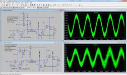
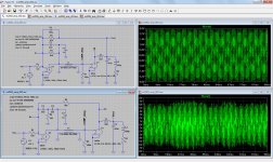
Here's a look at both principles in more detail with gain settings etc. being equal. The post filter feedback is Choco's basic version and the pre filter feedback is the defacto IRS2092 implementation I posted earlier with some of the circuit values changed to Choco's defaults.
For the post filter approach the switching frequency is ~400kHz (2.5us period) and for the pre filter approach the switching frequency is 300kHz (3.33us period). The pre filter clearly has larger switching residue at the output. Distortion @1kHz (for what it is worth) is ~0.60% for the pre filter and ~1.3% for the post filter arrangement.
Looking at the output, the post filter is much cleaner, with much better controlled output, than the prefilter. I'm going to assume this the effect of the post filter being in the loop, or, and that needs verifying, the loop around the pre filter isn't calculated properly and allows for more overshoot and ringing.
Unfortunately I don't have more time to tweak and/or try different things this afternoon as I have to run out for work, but I'll revisit this tonight/tomorrow, in the meantime comments and suggestions are always welcome.
Thanks for providing the groundwork, much appreciated.
Here's a look at both principles in more detail with gain settings etc. being equal. The post filter feedback is Choco's basic version and the pre filter feedback is the defacto IRS2092 implementation I posted earlier with some of the circuit values changed to Choco's defaults.
For the post filter approach the switching frequency is ~400kHz (2.5us period) and for the pre filter approach the switching frequency is 300kHz (3.33us period). The pre filter clearly has larger switching residue at the output. Distortion @1kHz (for what it is worth) is ~0.60% for the pre filter and ~1.3% for the post filter arrangement.
Looking at the output, the post filter is much cleaner, with much better controlled output, than the prefilter. I'm going to assume this the effect of the post filter being in the loop, or, and that needs verifying, the loop around the pre filter isn't calculated properly and allows for more overshoot and ringing.
Unfortunately I don't have more time to tweak and/or try different things this afternoon as I have to run out for work, but I'll revisit this tonight/tomorrow, in the meantime comments and suggestions are always welcome.
Attachments
Ssassen,
the enable swithc does not function. remember the current is flowing from gnd to a negative node, the Vin of the 7812 regulator. not simple to switch, try an optomos.
Noted with thanks, Vout will default to V- when Vin isn't connected, which obviously is not a good idea. I'll have to think of another solution, perhaps a LM317 with a transistor to reduce the output to Vref (1.25V)?
An externally hosted image should be here but it was not working when we last tested it.
@Choco,
... basic version and the pre filter feedback is the defacto IRS2092 implementation..
That is not making much sense.
To get a reasonable comparison you would need to go for the post filter feedback evolution with 2nd order integrator, like the defacto implementation of the IRS2092. Also you would need to adjust fs to become identical in both designs, because the amount of switching residuals is mostly related to the fs in relation to the resonance frequency of the output filter.
Then you have to tune both approaches to get the best of it. After all this you find just following differences.
- Dependency of fs vs signal level. However this difference will be less a general fact, but more a result of your chosen optimization.
- Post filter feedback will provide a wider bandwidth beyond the resonance of the filter and without peaking.
-Step response of post filter feedback design will be almost independent from load.
-Non linearities of the filter components will hurt less in the post filter feedback design, but often also do not hurt much in pre filter feedback designs.
- Damping factor of the amp with post filter feedback will remain high over entire audio range.
Both values appear much too high - especially with respect that this is still the system with ideal power comparator instead of MosFets.Distortion @1kHz (for what it is worth) is ~0.60% for the pre filter and ~1.3% for the post filter arrangement.
Have a look to your max allowed step size. For simulation of THD of a switch mode amp which is running at 300-400kHz your choice of 100ns is huge.
For THD simulation of such classD amps in LT spice you should limit the max. step size somewhere between 1ns...20ns. The better your amp, the lower you have to limit the step size. Otherwise the result will show the short comings of the simulation instead of the amp. Also your fuzzy carrier residuals are pointing into the direction of pretty some quantisation errors - like step size.
Once you have reached distortion levels of -80db including MosFet switching stage, then further optimization by sim does not make much sense anymore, because at such low THD levels the fit between sim and reality is not given.
Another thing to check may be Simulate -> Control Panel -> Compression -> Enable 1st Order. .option plotwinsize=0 is supposed to turn it off but I find LTSpice overrides with the default settings on each new start; annoying and contributing roughly 0.3% THD.
I typically run with something like the below. Haven't put much effort into finding optimum settings but they may be of some help as a starting point. Curious if others have refinements; in particular, Tstep = 0 may be questionable. .param fin is the frequency of the input sine for THD measurement in Hz and out is whatever the name of the desired node voltage is.
.tran 0 {15/fin} {5/fin} {1/(16384*fin)}
.option numdgt=15 plotwinsize=0
.four {fin} V(out)
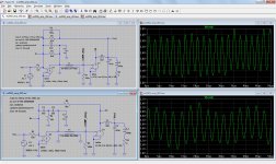
I guess you learn something new every day? I've been well versed in the art of simulating with LTspice, however never figured the timestep option made such a big difference with Class-D, for linear amplifiers I've been using the 100ns option for years and it has always proved to work just fine and the simulations would accurately represent reality in the majority of cases.
In retrospect it makes sense, as the 'ideal power comparator' I used can indeed do ns switching. I've rerun the simulations with a 1ns timestep and things are now making a lot more sense. Thanks for the suggestions and feedback gents!
In retrospect it makes sense, as the 'ideal power comparator' I used can indeed do ns switching. I've rerun the simulations with a 1ns timestep and things are now making a lot more sense. Thanks for the suggestions and feedback gents!
re enable:
a solid state relay is a simple solution to softly switch the negative voltages.
CPC1008N - CLARE - MOSFET Relay, 100 V, 150 mA, 8 ohm, SPST-NO | Farnell element14
a bit more than a euro..
ps you even can create aliasing effects with the timestep set wrong
a solid state relay is a simple solution to softly switch the negative voltages.
CPC1008N - CLARE - MOSFET Relay, 100 V, 150 mA, 8 ohm, SPST-NO | Farnell element14
a bit more than a euro..
ps you even can create aliasing effects with the timestep set wrong
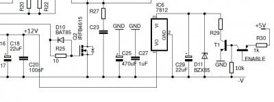
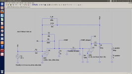
I've been rather busy at work, but did manage to squeeze in some time to take a look at housekeeping and cleaning up the schematic. Attached are the revised amplifier and the housekeeping schematic.
For the housekeeping I had a few things I wanted to implement:
1) Delayed startup with AC detection
This has been implemented with a 4093 quad NAND gate powered off of the negative rail. The latter makes interfacing with the IRS2092 and the floating 12V supply a bit easier.
I've opted to have the +5V/-5V supply for the IRS2092 come up right after powerup, which is what the datasheet stipulates. The CSD pin and the 12V floating supply will come up after ~2 seconds. The amplifier will then be ready to play music after the cap on the CSD pin has reached upper treshold, typically ~0.1 seconds after.
AC detection takes the two AC inputs from the transformer and makes sure that when the amplifier is switched off the CSD pin is pulled to -5V and the 12V floating supply is disabled. This should guarantee no squeeling or popping noises can be heard from the loudspeaker after the amplifier has been turned off.
2) DC Error
One of the things that kills a loudspeaker quickly is a large DC voltage across its input. I've implemented a DC error protection that will engage with DC voltages >6V by disconnecting the amplifier from its power rails and keeping it disconnected until power has been cycled. This way around any faults in the amplifier itself or the fuses failing to blow will not result in additional damage, unless the power supply itself is at fault of course.
I'm relying on the built in over current protection to detect any excess currents flowing due to a shortcircuit, or the amplifier being overdriven.
Anything I missed?
Attachments
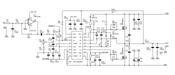
Alright, one of the tasks still left to do was to calculate the required resistor values for the over current protection. This is largely dependent on the MOSFETs used and the desired maximum current.
In my case I'll be using the IRFB4615 MOSFETs, which have a Rds(on) of 40mOhm and a maximum continuous current of 35A. For the sake of simplicity I'm going to go ahead and set the trip level to 35A.
Referring to the schematic in my previous post, R9 and R10 set the trip current for the low side over current protection (OCP). According to IRF's application note (AN-1138) these can be calculated given the following formula:
Vocset=Itrip*Rds(on)
Vocset=35*40mOhm
Vocset=1.4V
Vref=5.1V
R10=(Vocset/Vref)*10e3
R10=(1.4/5.1)*10e3
R10=2.7kOhm
R9+R10=10k (requirement)
R9=10-2.7
R9=7.3k
Closest E12 value is 6.8k, however that means that to meet the R10+R9=10k requirement, R10 will need to be 3.3k. That means Itrip will be different from calculated, so lets see by how much:
R10=3.3kOhm
3300=(Vocset/5.1)*10e3
0.33=Vocset/5.1
Vocset=1.683V
Itrip=Vocset/Rds(on)
Itrip=1.683/0.04
Itrip=42.1A
I guess with a Ipeak of 140A (pulsed drain current) on the IRFB4615, there's some margin (42A is 120% of 35A) so that's acceptable too.
High side current sensing is based on the measurement of Vds (Vdrain-source) across the high side MOSFET during high side turn on through pins CSH and Vs. An external reverse blocking diode, D2, is required to block high voltages from feeding into the CSH pin while the high side is off, hence the forward voltage (Vf) gets added to that voltage.
We'll set the high side over current trip point to the same value as we've set the low side over current trip point. To set the high side over current protection resistor values R11 and R12 need to be calculated given:
R11+R12=10k (requirement)
Vthoch=threshold voltage over current high side
Vthoch=1.2V
Vds=drain-source voltage at Itrip
Vf=forward voltage of D2
R12=10e3*(Vthoch/Vds+Vf)
Vds=Itrip*Rds(on)
Vds=42*0.04
Vds=1.68V (same as Vds on the low side!)
Vf=0.6V
R12=10e3*(1.2/1.68+0.6)
R12=10e3*0.526
R12=5.3kOhm
R11=10-5.3
R11=4.7kOhm
Picking E12 values, we'll select 5.6kOhm for R12 and 4.7kOhm for R11. This will set the Itrip for the high side to 38A, that's 90% of the low side overcurrent trip point, so I guess that's acceptable.
The next item on the list is selecting the dead-time setting.
The IRS2092 comes with a range of preset dead-time settings, which can be selected using a combination of resistors, R13 and R14 in this case. The selection available is between 25 and 105ns. From looking at the various IRF reference designs, and some of the suggestions in the application notes, the DT2 option, 45ns, seems to be the most used setting, resulting in 8.2kOhm for R14 and 3.3kOhm for R13.
I'm going to assume that's safe to use, as any additional dead-time can be added by gate stopper resistors with the defacto diodes over them. Or, when needed, a different selection for R13/R14.
Thoughts?
Last edited:
8.2k\3.3k results in DT3 option 75nsthe DT2 option, 45ns, seems to be the most used setting, resulting in 8.2kOhm for R14 and 3.3kOhm for R13.
For your 5615\4615 mosfets , the best choice is DT3 75ns and 10Ohm in gates without any diodes.as any additional dead-time can be added by gate stopper resistors with the defacto diodes over them.
Thoughts?
Other combinations give a shootthrough.
For the 4227 mosfets - DT4 105ns and 4.7Ohm in gates .
Made and tested in about 50pcs of 2092 based amps.
- Status
- Not open for further replies.
- Home
- Amplifiers
- Class D
- Tips and suggestions on IRS2092 implementation?