@Sassen
You will find input referred noise of OTA specified with 250uVrms.
A good class AB IC amp yields 1uVrms.
I never saw any class-d-amp with significant less noise.
Btw, in the 90s I experimented with class-d. Noise was a concern and depended solely on the quality of the comparator. LM393 and the likes were a no-go.
Eventually I found some very fast OP-amps from Maxim that did a much nicer job.
For other issues like optimal dead-time timing and short-circuit-proof design I never found a smart solution.
Nowadays I go for TI-class-D, solving my headaches, and the additional noise level is of minor concern if you select the lowest gain setting.
Just my 2c
Last edited:
Yes, another reason for using external NPN/PNP is that the driver IC already gets hot by itself before counting losses due to gate output currents.
The ZXGD series (also ZXTC) is a good idea from Zetex/Diodes, a fast (high hFE up to high Ic) NPN/PNP combo advertised as gate driver (also with high e-b zener voltage). The IR ICs drive these buffers well, a low value resistor is recommended between the bases and the driver IC, with three purposes, 1st is to tame reverse transistor effect when it gets activated by gate transients (due to parasitic Lsource, usually negative spikes up to a few volts), 2nd is to reduce current demand from driver IC during gate transients exceeding the rails (to push IC latch-up due to reverse currents far from operation point), and 3rd is to get potential fuse effect to save driver IC. Another improvement seen in ICs like IRS20957 or IR2092 with NPN/PNP buffers happens because the transistors that pull the outputs of these ICs high are N-ch FETs (Vgs-th is around 1.2V), this in practice slows down the last half of the rising of Vgs and in most cases prevents it from reaching gate drive voltage rail. With the buffers and its associated b-e charges, Vgs is usually allowed to reach the rail because the NPN BJT keeps ON for some more time after the high FET of the driver IC cuts off. Actually I place zeners at the outputs of these IR ICs to get "locally regulated" gate voltages, taking advantage of that medium-high Z zone when outputs are almost high. For other purposes like SMPS it's better to pick driver IC whose outputs have P-ch FETs driving them high without this upper "dead band".
The MIC4420 accepts a weaker input signal at the expense of costing about 3 times more, like for being driven from a microcontroller or from logic gates, I find more use for ICs like that in SMPS. Also, the MIC is likely to produce higher di/dt EMI spikes than the NPN/PNP combo (which has a smoothing effect due to b-e charges).
I think there is an IRS209575 on this amplifier: 6moons audio reviews: SPEC Corp. RSA-M3EX
or here:
SPEC RSA-M3 EX Real Sound Amplifier
Expensive 🙂
Maybe the pictures are not so clear to my eyes...
or here:
SPEC RSA-M3 EX Real Sound Amplifier
Expensive 🙂
Maybe the pictures are not so clear to my eyes...
Going forward, does anybody have a LTspice library for the IRS20954/955/957? I'd like to try a few options in the simulator with a (semi)discrete frontend to get rid of the (somewhat) noisy OTA on the IRS2092.
I can show the LTspice simulation circuit that I use for IRS20957 and IRFB4615 output stage, it is intended for quickly simulating the stuff that matters (propagation delay, dead time), not as an ultra-accurate model taking hours to run. Actually, main purpose of this circuit is modulator simulation and fine tuning, since designing around the IRS20957 is quite straightforward.
It also includes current limiting to analyze possible interaction with output filter and the whole amplifier loop. Current limiting OFF period depends on capacitance attached to CSD pin, the value modeled (15pf) represents some IC capacitance plus some PCB capacitance from a 10 mil trace similar in length to the IC itself plus some collector C from a small BJT. Hard to get lower figures in practice. Too long period can excite output filter close to resonance, without the modulator being able to control it, as obviously current limiting overrides PWM input.
The modulator has been "censored" because this is part of a commercial design, I cannot show it all.
Attachments
@Eva,
Thanks, I'll have to give that a try, although I might ping you with questions via PM as the complexity of what you've drafted is a little beyond what I typically use LTspice for (loop-gain, freq. response, that sort of stuff).
Any thoughts on the noise issue I commented on in my previous reply? Has that got merit, or would a (semi)discrete approach make sense? I'm thinking along the lines of a OPA860 for the OTA and a LT1016 for the comparator.
Something I have learned with time is that a minimum degree of complexity is required in order to produce universal designs, those ones that can be successively used as building (or teaching) blocks (because they suit practical needs matched to the world), while allowing to permanently unload from the brain most of their related complexity. Something like "dealing with some more complexity now to allow dealing with less complexity later".
Regarding the goal of an universal design I fully agree.
Regarding teaching I agree with the adder that this teaching expects already well educated pupils.
Regarding 'matched to the real world' you have to restrict it to the real world of professionals. But it does not at all match to the real world of classD DIYers.
The key learning from my 2kW thread was that such a design is simply too complex for most people and can be reproduced only by very few DIYers.
The key learning from my LiteAmp is that even this is too complex.
BTW: Welcome back !
The charming thing of the IRS2092 is that it allows low complexity, but is flexible and scalable in power.I read through your 'SystemD LiteAmp' topic which proved to be an excellent read although one of the things that did stick out like a sore thumb is your comments on the noise contribution of the OTA in the IRS2092 to the S/N ratio of the whole amplifier. I remember designing and building a UcD style amplifier back in 2005 (yes, we're getting old indeed!) with the TDA8939, which I ultimately scrapped due to the built in comparator being rather noisy, I'd rather avoid a repeat exercise.
Would selecting the IRS20957 rather than the IRS2092 be a better choice here in terms of amplifier S/N ratio? It would obviously require a larger number of parts to construct the amplifer, as the OTA has now got to be built up externally, either using discrete parts or ICs.
Regarding noise you have to use large input signals. If you design the power amp with low voltage gain and use input signals larger than 5Vp for clipping, then you can achieve reasonable results. For calculation simply use an input voltage noise density of 50-60nV/sqrt(Hz). If your design shows more noise than what you get from this calculation, it indicates that you are suffering from layout short comings.
Of course when going for a pure half bridge driver & external comparator & external amplifier you get all degrees of design freedom for a higher performing solution.
For simulation of a half bridge driver of your choice you can modify the simulation model, from the LiteAmp. Skip the OTA. Adjust the halfbridge driver section according to the data sheet of your half bridge driver. Kick my feedback loop + modulator and place yours.
This thread so far covers the input stage and gate drive, but misses out the power stage.
When going for power, especially with MosFet that can handle more than 150V, then it is worth to look into the halfbridge configuration.
In order to show why I am attaching some measurements with the IRFB4227 running from +/-80V and handling 20A load current at the same time.
This is the most demanding situation for the low side MosFet at large signals during the negative half wave of the output signal.
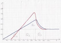
First picture shows the entire HF period.
Second picture shows a zoom of the turning on with 50ns/div.
Third picture shows a zoom of the turning off with 50ns/div.
The upper trace always is the drain current of the low side MosFet. Scale: 10A/div.
The lower trace always is the drain source voltage of the low side MosFet. Scale: 50V/div
The heavy current peak upt to 38A during turning on is not a shoot through, it is caused by the Qrr of the body diode of the opposite MosFet.
The related losses are high. During the time which is need to take over the load current (ramp from 0-20A) and for the first part of the removal of Qrr (ramping from 20A-38) the Vds remains almost at full rail-rail level. Switching losses at 280kHz plus conductive losses sum up to 100W if you would apply this as a continuous DC load situation. Fortunately this happens to each MosFet only during a short time of each audio signal period. Also the self oscillating designs reduce fs at large signals, last but not least audio signals usually come with high crest factor. Over all it will work for audio if sufficient cooling is provided. But from perspective of power electronics design it is a poor solution.
How to improve?
1) Just apply a stronger gate drive:
Not clever. The reverse recovery peak is getting larger when you go for higher di/dt.
2) Apply a stronger gate drive and reduce dead time:
For IRFB4227 that's reasonably possible for currents up to 10...15A. If you manage to control your devices very precise with very low dead time or even some overlap then there is simply no time to charge much of Qrr in the body diodes.
However you must ensure that the hot RdsON multiplied with the current is smaller than the forward voltage of the hot body diode (==> For IRFB4227 I would trust up to 10A, may be 15A).
Difficult point is that you really have to know how to handle the nano seconds.
Furtheron you will suffer from higher idle losses, because you will not have ZVS at idle condition - except you go for adaptive dead time.
3) Consider the old school arrangement: A series shottky connected with its cathode to the drain (avoids that the body diode becomes conductive) and a fast diode from MosFet source to the anode of the shottky (re-enabling of a reverse path).
Disadvantages: Triple amount of power devices. More complex PCB design.
4) SiC
5) GaN
For inspiration regarding 3) you can have look to my 2kW thread.
V1.5 of this amp is still my very favorite in terms of performance and sound.
Of course also for this amp there are improvements possible.
I.e.:
- Implementation of a cycle by cycle current limitation at moderate overcurrent instead of only shutting down at massive over current.
-Or going for fully differential signal handling like Bruno is now promoting with his N-core and like Eva is doing since ten years ..and I saw some thread of a russian guy here who also does.
- ....
Attachments
Actually: total reverse recovery losses (body diode plus opposite FET) are reduced as di/dt is increased. This can be pushed to the point where the body diodes latch up, less some reliability margin. Of course layout requirements increase. I think the well known FETs currently available up to 200V d-s are OK without any extra diodes, heat losses are manageable. I designed a 6KW module that has been selling for years now.
Of course, after the power challenge, one of my fields of research has been:
Signal integrity analysis in class D amplifiers:
- Structural noise: resistor V noise, op-amp V & I noise, comparator V & I noise. This can be analyzed as in linear amplifiers.
- Dynamic noise: when using any good fast comparator (like TL3016), any hysteresis amplifies any noise at its inputs, even hysteresis from unmatched layout sub-pF capacitances from comparator output(s) to input(s) has a measurable effect. On the other hand, any parasitic negative FB results in bounce. Optimum solution is to adjust PCB layout for slightly higher positive FB parasitic capacitance in comparator, just the minimum to suppress bounce. Compact multi-channel layout requires multi-layer PCB and ground planes. Expanded single-channel layout can do with 2 layer and clever use of distance. One or more FB poles at a few Mhz recommended (one adjusted to compensate output capacitor inductance, the other can just be the few pF of parasitic GND capacitance at comparator inputs).
- Self destructing:
# Parasitic resonant elements in power stage or output filter radiating EMI strong enough (or corrupting FB signal enough) to cause comparator bounce. The amplifier finds oscillation modes at frequencies higher than the one determined by phase shift and delay elements.
- Self interference:
# Square wave to FB sine: Causes comparator hysteresis or bounce depending on parasitic polarity. Hysteresis results in increased noise. Bounce results in increased noise and reduced reliability. Increased THD due to distorted FB sine. Square wave can come from output inductor leakage field picked up by PCB traces. Measurable even with ground plane, depends on distance.
# Spikes to FB sine: Causes random premature or delayed toggle of comparator. Increased noise and THD. Spikes can come from commutation processes in the own channel delayed w.r.t. comparator toggle.
--> Balanced signal processing and good layout can cancel most of this, even in compact designs.
- Channel to channel interference:
# Audio to audio: like parasitic capacitance from output of one channel to op-amps of another. Undistorted cross-talk, mostly harmless.
# FB sine to FB sine: Causes moving bumps in noise floor that go higher freq and worse as DC offset mismatch in channels increases, or as Fsw mismatch increases. Causes increased random noise when channels play uncorrelated signals.
# Square wave to FB sine: Causes harmonic sprays in noise floor.
# Spikes to FB sine: Increased noise and THD.
# Bullying: Mismatched amounts of parasitic coupling: 2 or more channels get parasitically synchronized and cause increased interference to a 3rd channel, w.r.t. what would be caused be uncorrelated sources.
Last edited:
total reverse recovery losses (body diode plus opposite FET) are reduced as di/dt is increased. This can be pushed to the point where the body diodes latch up, less some reliability margin. Of course layout requirements increase. I think the well known FETs currently available up to 200V d-s are OK without any extra diodes...
I wish you would have said the total turn on losses are reduced as di/dt increases.
But regarding Qrr things definitely do not get better with increasing di/dt.
Lets focus on the switch which has to remove the Qrr, because this switch is seeing the massive overlap of current and voltage, while across the diode the voltage remains comparably moderate during most of the time when it is carrying current.
In the attached drawing I have put two situations.
First the drain current as shown in the screen shot of my previous posting with very moderate di/dt of 500A/us, showing the current in the switch which is being turned on hard.
Second - the situation with double di/dt.
Q1 is the amount of charge until the switch has taken over the load current.
Q1 decreases with increasing di/dt. That's fortunate.
But after Q1, still the body diode of the other switch is flooded with its Qrr.
During the time of Qrr the switch has to carry the load current plus the reverse recovery current peak. Q2 which simply results from trr and the load current does get moderately less, but just moderately, because trr decreases just moderately with higher di/dt. Qrr unfortunately increases with larger di/dt.
Q3 starts earlier and ends earlier at higher di/dt, so not much of a change.
In sum the reduction is mostly related to Q1 which is not the T.rex of the show (except when operating at very low di/dt).
With devices like the IRFB4227 reasonable di/dt are in the range 500A/us...1000A/us.
But already at 1000A/us without fully optimized dead time you are buying a small reduction of losses by a remarkable current peak and the related increase of EMI.
Yes, for audio such approach will work, no matter if I like it or not...heat losses are manageable. I designed a 6KW module that has been selling for years now.
Personally I decided for 200V devices or higher and at the same time handling load currents above 15A, to go for the right circuit and/or semiconductor technology.
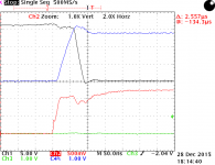
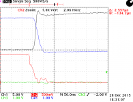
Then you can get switching behaviors like shown in the next screen shot.
This is a modified LiteAmp running from +/-82V and delivering 30A into the load.
The effect of Qrr is almost neglectible, di/dt is kept moderate (fortunate for EMI). Losses are moderate.
Don't clompain about the small voltage overshoot, it is related to the current probe which adds inductance to the drain connection.
Ch1: Vds of low side switch, 50V/div.
Ch2: Vgs of low side switch, 5V/div.
Ch4: Id of low side switch, 10A/div.
P.S.
True, latching can become an issue and I am wondering why many of the MosFets, which are being promoted for classD do have no dv/dt specification.
Fortunately IRFB4227, IRFB4615 and IRFP4668 are positive excemptions...
P.P.S. Yes, I got a X-mas present. A vintage Tektronix storage scope. 🙂
In future I can always provide such nice multi colored pictures and properly triggered events including zoom etc.
Attachments
Last edited:
...when using any good fast comparator (like TL3016), any hysteresis amplifies any noise at its inputs...
Good point! I did not dig into this mechanism yet, but now reading your hint...
...yes, makes sense.
Yes, of course the improvement comes from what you call Q1, diode recovery only takes substantial time when output current is already high. On the other hand, the di/dt process is in the signal path, it increases output impedance, Fsw drop near clipping and high level THD. Now I'm working in something with 4 layer main PCB and 6 layer daughter PCB, where the di/dt limiting factor are the FETs. A quick output impedance measurement was in the <.005r range with no substantial HF rise.
The challenges I have been facing are more signal-integrity related, like packing 4 half-bridge channels (of something with 70V and 90V +/- rails version, bridgeable, full protections, VCA limiter, adjustable negative resistance), 2 flyback power supplies and 2 MCUs (with UARTs and I2C communications) in very little space, and getting mid-level THD <=.01%, 10khz cross-talks in the -90dB range and SNR >=110dB.
Here it seems the good stuff has been kept alive and accurate, but I feel that not many new learning curves have been climbed meanwhile. I have been climbing plenty. From developing MCU communication protocols, to developing a clamped gyrator LPF with a gate drive dual NPN/PNP giving >50dB rejection to the ground current frequencies in the few khz range resulting from MCU algorithms modulating MCU current consumption...
Thanks gents for the insightful replies, much appreciated.
Let me illustrate what this amplifier will be used for, so the requirements I mentioned in the first post will start to make more sense.
I'm currently designing a new loudspeaker which will use high-efficiency mid and treble drivers (~95dB), but will be paired with two bass drivers that lack the required efficiency (~85dB) to be able to use a passive crossover without sacrificing overall loudspeaker efficiency. So the idea is to drive the bass drivers with an active crossover and an amplifier to compensate for the ~10dB efficiency difference between the drivers (and allow for some other fanciness which isn't easily accomplished with a passive crossover).
Amplifier output requirements
The tentative specifications I posted in the 1st post of this topic detail an amplifier capable of delivering 500-800W into a 2R load. The 500W rating would be an nominal rating, whereas the 800W rating would be a peak rating. How do I arrive at this number some of you might wonder?
In this particular case I'll be using the amplifier to drive two 4R bass drivers in parallel, hence the 2R requirement. The combined 4R bass drivers have about 88dB/1W/1m of sensitivity (two 85dB/1W/1m drivers combined see a 3dB increase in output). If I set the maximum level for music playback to 125dB a total of 37dB of gain is required. If I want to drive these to an ear bleeding 125dB this is 70 times louder than the 1W playback level, which brings the total to 70W.
However I plan on adding Linkwitz transform (Active Filters) to allow bass extension all the way down to 20Hz with a favorable Q. Linkwitz transform allows you to take a driver in a sealed enclosure that has a fixed Fc and Qtc for that volume, determined by the driver's T&S parameters, and lets you 'transform' or rather simulate a new Fc and Qtc for that driver at the expense of driver excursion and required amplifier output. In this case I'm going to need some extra headroom on the amplifier, anywhere from 6 to 12dB, hence four or eight times the required amplifier output, which means we're looking at 280 to 560W total.
Power supply requirements
So with those requirements lets calculate the requirement for the power supply:
R=V/I (Ohm's law)
P=I^2*R but also P=V*I hence:
P=V*I=I^2*R=V^2/R
P=560W
560=V^2/2
V^2=1120
V=√1120
V=33.5V
The above value is correct if we were to put DC into our 2R load, however amplifier power ratings are not DC, but RMS, hence relative to a sine wave into the load. So we need to calculate the RMS value, which is simply the amplitude of the sine wave (33.5V in our case) multiplied by √2.
Vrms=V*√2
Vrms=33.5*1.41
Vrms=47.2V
If we take into account losses in the MOSFETs and the voltage sagging under load then +/-55V rails will be a suitable supply voltage. Now lets look at how much power the power supply needs to be able to deliver.
If we assume a 90% efficiency for the amplifier and the 560W/2R nominal rating for output power the DC rating would be 622W. However the RMS rating would be higher, by a factor of √2 to be exact, which then puts our rating at almost 900W. This a somewhat simplified calculation, based on the assumption we'll be playing a single sine wave at full power.
Another way of looking at this is considering the crest factor (http://en.wikipedia.org/wiki/Crest_factor), as obviously an amplifier will be used for music playback, not the reproduction of sine waves. A typical classic music recording has a 20dB crest factor, this simply means the peak power of the recording is 100 times higher than the RMS power. Typical rock or heavy metal, or anything that'll be played on the radio (with compression), sees about a 3-6dB crest factor. On average, and this has been verified by comparing 4500 tracks ('Dynamic Range' & The Loudness War), the crest factor is around 14dB.
So with a 14dB crest factor the power requirements are relaxed quite a bit, as the peak power is now about 25 times more than the RMS power. In our case, as this will be used for audio playback in the living room, a power supply rating between 250 to 500W will be sufficient. As we'll never be running the loudspeakers at 125dB for any prolonged period of time. Frankly, and this is a personal preference, I find anything upwards of ~100dB too loud to listen to comfortably.
Hence a ~300VA toroidal transformer with about 40.000uF of buffering will provide enough power to allow for 70W RMS or, when 6dB of gain is added for the Linkwitz transform, 280W RMS and will also be able to provide more power for short periods of time.
MOSFET selection
Assuming the worst case scenario, where we have to drive 560W into a 2R load, the current required to accomplish this is:
P=I^2*R
560=I^2*2
I^2=280
I=√280
I=16.8A
Considering we'll be using the IRS2092 to drive the MOSFET we'll need a MOSFET with a low gate charge/capacitance if we want to drive the MOSFET directly. I was unable to find any exact references to what the maximum gate capacitance is the IRS2092 can drive, but from the documentation and forum posts floating around the web it would appear that anything over 50nC/2nF requires extra gate drivers.
With the +/-55V rails on the power supply, the BVdss (drain-to-source breakdown voltage) requirement needs to be at least 150V, 120V would be cutting it too close, especially when ringing or overshoot is factored in.
The gate charge Qg and input capacitance Ciss need to be as low as possible, as that would make the MOSFET easier to drive and reduce losses on the IRS2092.
With those parameters being key in MOSFET selection I found three MOSFETs that seem to fit the bill:
IRFI4020H - 5-lead isolated TO220
http://www.irf.com/product-info/datasheets/data/irfi4020h-117p.pdf
This is a single package 5-lead isolated TO220 that looks to fit the bill, apart from the maximum switch current, which is at 9.1A. If the 560W/2R peak power requirement is relaxed, this could be a suitable MOSFET, you gotta love the simplicity.
IRFB4615 - TO220
http://www.irf.com/product-info/datasheets/data/irfb4615pbf.pdf
There isn't a checkbox left unchecked with this MOSFET really? 35A source current, low gate charge and input capacitance, low Qrr, etc. Only thing I would've liked to see is an isolated TO220 package.
IRFB5615 - TO220
http://www.irf.com/product-info/datasheets/data/irfb5615pbf.pdf
Slightly different specifications than the IRFB4615, but only marginally so. Furthermore the datasheet details this has 'key parameters' optimized for class D, am I considered gullible for thinking that on that basis this indeed could be better than the IRFB4615?
Thoughts?
Thoughts...
Your considerations for the PSUdo not really fit IMHO.
What do you mean with PSU power would be a rms rating?
RMS is just a math help applied to currents and voltages in order to make
power calculations easier in linear systems.
The wording of xyz Wrms was only introduced to differentiate power from misleading advertising power names and ratings. But basically the power is not a root mean square (that's only making sense for the currents and voltages), but an average power derived from the integral of the instantanous power p(t) over one period, divided by the period.
When looking to instantanous power p(t) it will be sine^2 function. Means it has double frequency of the voltage, contains negative values only in case of reactive load and can reach max values of twice the power P.
With a classD amp this p(t) will be seen just increased by amp efficiency at the PSU. Means you supply load current will be a strongly modulated current following a sine^2 function, even when playing a pure sine.
Transformer rating and drop of supply rail:
Transformer ratings are done for linear loads which draw sinusodial currents from the transformer. But with the rectifier and large caps your transformer has to deliver the entire charge within short time slots. As a consequence of the rectifier, the transformer can only deliver charge to the capacitors in the short times when the output voltage of the transformer exceeds the capacitor voltage. ==> The transformer is working short and very high current peaks, resulting in high rms current its windings.
But as you mentioned, music is not a continuos signal...
It depends on your usage whether the 300VA transformer will be sufficient.
Usually yes, personally I would chose a 500VA.
Sagging:
From experience a +/-55V rail, sized as proposed by you will sag more than you expect. Reaching 500W / 2R is very optimistic.
BTW: Are you sure about your Vrms?
MosFets:
The IRFB4615 definitely can be recommended. Data sheet is good and
on my bench it was also performing fine (Well, finally I killed it when operating from +/-62V and delivering 30A with 500kHz fs, but with 250..300kHz it should be fine for 2R from a +/-55V rail.)
The IRFB5615 is exactly one of the types promoted for
classD , but without dv/dt specification. Very ignorant way of specifying a
MosFet for any hard switching application.
Most likely the IRFB5615 is just a spin of from the IRFB4615 will be able to handle high dv/dt, but the data sheet of the IRFB5615 is insufficient for the target application....
The dual MosFets IRFI4xxx are also nice ones, but as you already highlighted, they are too weak for your application ( and they are also specified in the ignorant way without dv/dt rating).
.. I feel that not many new learning curves have been climbed meanwhile..
Don't bother. People can't stop loving you - even if you tell them, that they are boring.

@Choco,
Thanks for the feedback.
Could you perhaps illustrate how you would approach this given the requirements for the amplifier? I'm used to working with linear amplifiers, the last time I fiddled with a class-D was 11-years ago, on this very same forum I might add, see here:
http://www.diyaudio.com/forums/class-d/58476-my-non-discrete-sodfa-class-d-amp.html
Can't the dV/dt be calculated from the other specs? They do specify td(on) > turn on delay time, tr > rise time, td(off) > turn off delay time and tf > fall time? And to ask a perhaps more meaningful question, what are we looking for in dV/dt, is there a specific range it should be in?
Thanks for the feedback.
Your considerations for the PSUdo not really fit IMHO.
Could you perhaps illustrate how you would approach this given the requirements for the amplifier? I'm used to working with linear amplifiers, the last time I fiddled with a class-D was 11-years ago, on this very same forum I might add, see here:
http://www.diyaudio.com/forums/class-d/58476-my-non-discrete-sodfa-class-d-amp.html
BTW: Are you sure about your Vrms?
... The IRFB5615 is exactly one of the types promoted for classD , but without dv/dt specification.
Can't the dV/dt be calculated from the other specs? They do specify td(on) > turn on delay time, tr > rise time, td(off) > turn off delay time and tf > fall time? And to ask a perhaps more meaningful question, what are we looking for in dV/dt, is there a specific range it should be in?
Step 1:..how you would approach this given the requirements for the amplifier?
Set up a simulation with your transformer, rectifier and E-caps.
Load it with two simple resistors dissipating in total 560W.
Watch the currents in the transformer and rectifier and also watch the sagging.
Step 2:
Modulate the load with a sine^2 function and apply this intermitting to pos and neg rail.
Step 3:
Put a real switching stage as load and see all details of bus pumping.
But this is most likely not much headache with your large caps, feel free to skip.
Step 4:
Superimpose a slower duty cycle to your load, according the rythm and crest factor of your expected music.
A short cut could be to do just step 1 and 4.
Note:
Signal contents in the region of the natural resonance frequency of the closed sub will draw substantially less power, because there the impedance of the speaker is high. Linkwitz transform will not break up this phenomenon, but will work perfectly fine from accoustic perspective.
No, the worst dv/dt at full load in your application will strongly depend on your gate drive & layout and a little bit on your snubbering. Usually the most critical moment is the sloping of the half bridge at the end of the body diode reverse recovery at max load current. If this dv/dt is too high a parasitic BJT in the MosFet will be triggered and can cause defects.Can't the dV/dt be calculated from the other specs? ... what are we looking for in dV/dt, is there a specific range it should be in?
As a rule of thumb for classD you can watch out for dv/dt specs of 15kV/us or higher.
I can follow your numbers to some point...
10^((125-88)/20)~=70W
6~12dB Linkwitz transform gain means 4 to 16 times more power, +9dB is already 8 times more power. This gets into the 500W range.
Then we have to look at the power handling of the drivers. My definition of overkill is sizing a power supply much heavier than the voice coils can handle. I reached this definition burning some speakers and getting exhausted of moving heavy amplifiers. Loud LF has healing properties, it is going to be used at some time or another. Later I developed an amplifier with rms output current limiter. Now I'm developing voice coil temperature sensing without extra elements. What does this mean? Any higher long term power handling in power supply than in voice coils is just never going to be used, except the day speakers are damaged, so it is a myth, and in newer technology the myth is being phased out haha
So what is the power handling of the drivers?
infineon just came out with this one BSC093N15NS5 , only 9mohms, 33nC, but so8, need pcb as heatsink.
http://www.infineon.com/dgdl/Infine...n.pdf?fileId=db3a304319c6f18c0119cd1cc23279be
http://www.infineon.com/dgdl/Infine...n.pdf?fileId=db3a304319c6f18c0119cd1cc23279be
https://www.google.de/url?sa=t&sour...yRW57PQIuDx1druiw&sig2=2DBQMh-R3ynVQe8cdmRB4Ainfineon just came out with this one BSC093N15NS5 , only 9mohms, 33nC, but so8, need pcb as heatsink.
http://www.infineon.com/dgdl/Infine...n.pdf?fileId=db3a304319c6f18c0119cd1cc23279be
Correct PDF link
- Status
- Not open for further replies.
- Home
- Amplifiers
- Class D
- Tips and suggestions on IRS2092 implementation?