@Eva,
Thanks for the suggestions.
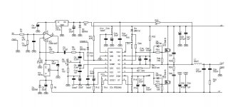
For some reason the forum keeps deleting images which I've uploaded as attachments and then linked to in the actual reply. Please find the image I posted in #48 attached, as well as my first attempt at the brute-force approach you've suggested.
Comments are obviously welcome and appreciated!
Thanks for the suggestions.
For some reason the forum keeps deleting images which I've uploaded as attachments and then linked to in the actual reply. Please find the image I posted in #48 attached, as well as my first attempt at the brute-force approach you've suggested.
Comments are obviously welcome and appreciated!
Attachments
Housekeeping:... I would also include DC protection with output relay ...
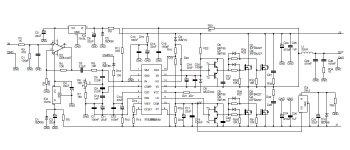
I plan to do this in similar fashion as we've done with the ExtremA design, i.e. shutting off the supply (latching) rather than a relay on the output. See below noted link for more details and schematics, obviously this will be modified for a half bridge rather than a full bridge.
ExtremA, a reference class-A DIY amplifier. - Concept and design
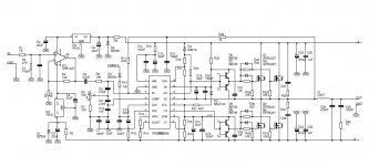
C23,C24,C25,C26 should have their center node connected to gnd, not to the output
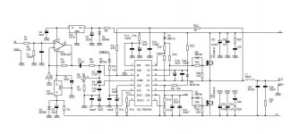
You're absolutely correct, what was I thinking? I must be getting old? Corrected schematics attached.
Attachments
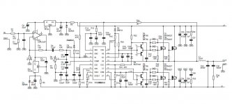
but the RC snubbers would be needed from the output to the rails. too bad the component numbering is different for the same parts in both schematics. anayway in the buffered gate drive version it's R32C27 and R33C28.
but the RC snubbers would be needed from the output to the rails. too bad the component numbering is different for the same parts in both schematics. anayway in the buffered gate drive version it's R32C27 and R33C28.
Thanks, I guess I was a little too quick with editing the previous version. Corrected schematics attached.
Attachments
The brute force approach results in high use of natural resources for leisure applications, or even worse, the proliferation of cults to natural resource waste. So the brute force approach is unreliable, not in the sense of losing function with time, but in the sense of making the whole world in which we live unreliable!! haha
...your diplomatic way of making friends with audio folks and SUV drivers is stunning. 😀
Or should I say: Making friends with - so called - homo sapiens?
This animal is really going the extra mile in order to waste its resources and destroy its environment until it starves to death.
And I'm glad no-one else noticed the other mistakes, perhaps I shouldn't be drafting schematics whilst doing other stuff, they say men can't multitask well, not sure whether that qualifies as an excuse though?
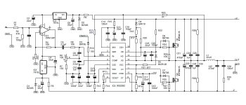
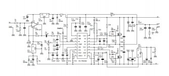
Frankly I just need a (long) vacation, I've had too much on my plate the last couple of years. Anyway, here's the latest, 12V floating supply for the IRS2092 thrown in for good measure.
Thoughts?
Frankly I just need a (long) vacation, I've had too much on my plate the last couple of years. Anyway, here's the latest, 12V floating supply for the IRS2092 thrown in for good measure.
Thoughts?
Attachments
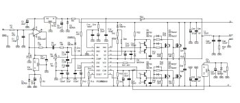
C31 gnd and D10 gnd should be -V
vakantie?
Thanks, fixed schematics attached once more.
Attachments
Of course these gate drive ICs are all intended to be driven from some kind of logic that, at least, checks the rails. No class D loop will behave at very low rails because the amplitude of carrier at comparator inputs decreases linearly with rails, to the point where parasitics take over. The simplest possible logic is to derive the VAA and VSS rails in such a way that this section of the IC enters UVLO before the amplifier starts misbehaving as rails drop at power off (ressitors from HV rails, small value capacitors, maybe draining resistors too). In my current project there is a 100 pin 100Mhz PIC32 doing complete supervision of 4 half bridges, including too short and too long PWM pulses, adjustable clip limiter, also limiting in case of excessive supply pumping and other incidences, etc. MCUs are useful for implementing full-reliability no-safety-hole housekeeping without lots of parts.
I'm not sure complete supervision can be fully trusted. firmware contains bugs, requires updates and are subjected to deployment issues, (custom boot-loader, version tracking)
Dont get me wrong I am all for a MCU supervision monitor system. makes 3rd party servicing only attractive and favourable to the original author of the design. (unless you sharing the firmware with your client)
I was going over an Agilent power supply lab power supply and they use a 8051 MCU, however I noticed supervision still used an analog system.
BTW PIC32 is great, I take it you off the PICKIT2 and using an ICD3
Last edited:
The internal stabilisation of IRS2092 for VAA and VSS is pretty poor.
If these voltages drop too low before the driver supply drops, then you can get sirene sounds after you turn off your PSU.
This can covered by three ways:
a) Add an analog supply monitoring circuit like the IRAUD7 reference design.
b) Add a uC for monitoring the supply like Nigel has done. This is attractive if you already use an uC in your design for housing keeping.
c) Ensure stable VAA and VSS until the point the UVLO of the driver supplies will turn OFF the MosFets. In my measurements stable VAA and VSS also were helpful for perfomance.
In your schematic you are connecting D4 just somewhere to the rail.
In the layout you should make sure to connect it close to the drain of the high side MosFet. Otherwise the high side overcurrent protection may start phantom tripping due to noise.
Admin feedback: I wrote a long technical post. I hit the "back" function of the browser by accident (in firefox: backspace without the focus set on a text object). No warning dialog. All text lost. After 13 years, basic forum issues imposing a *penalty* on people writing long and detailed technical posts remain unsolved. Nowadays almost every webpage with text input shows a warning dialog when text not posted is going to be lost. This is one of the various discouraging factors found when using this forum site. Now using text editor.
-----------------------
I think bassreflex has pointed out all the obvious issues with the circuit. Lets go with the not so obvious issues and shortcuts:
- Input op-amp: Datasheet states 4~5mA quiescent supply current. Load current is not going to be significant. I would just use two resistors, two zeners and two 100n caps for op-amp supply rails (or external +/-15V). When having a gain op-amp at the audio input of a power module I would always go for a balanced input (40dB CMRR typ. from 1% resistors). This is because when associating multiple class-D modules (and maybe an input board, all with its HV and/or LV supplies) inside an enclosure it is quite easy to create ground loops and magnetic interferences in wiring, and the practical cost of removing these effects may be higher than just adding the balanced input, even when the signal comes from an input board with another balanced input to the outer world. Once I saw QSC using balanced internal signal distribution in his big amplifiers, and adopted it.
- IRS2092 supplies and UVLO: Datasheet states 0.5~2mA (VAA/VSS) current with IC OFF, and 8~11mA with IC ON. (VAA-VSS) UVLO ON threshold is specified to be 8.7V and UVLO OFF 8.2V. Internal zener clamps spec is +/-7V. At least with some ranges of component values this is going to produce a motorboating effect at power OFF, particularly with high bulk capacitance in HV rails and the supplies for IRS2092 derived from these with resistors ("long screech complain of nature" in return for over-simplification). When (VAA-VSS) goes below 8.2V the IC turns off and VAA/VSS current drops a lot, this causes (VAA-VSS) to increase back and turn the IC on, cyclically (resistors to HV act as current sources, forming an oscillator with phase shift from local deocupling caps and UVLO hysteresis). IR is usually quite optimistic in their sample application schematics, more elements are always required for cleaner operation. Actually IRS2092 is designed to run on +/-5V external rails.
- Post-filter feedback: I have not ran simulations or developed topologies with IRS2092, but I think this schematic already has enough elements for implementing post-filter FB. Maybe for a second version. Pre-filter FB linearises switching stage, but inductor resistance appears in series with output. There is also variable peaking at HF, not an issue for LF applications.
- CSD: Charge and discharge currents are spec to be (+/-)100uA (+/-30%). Initial excursion is going to be 10V (70% of +/-7V). With 22uF this results in a 2.2s first ON delay. The paralleled 100nF capacitor at this location is a bit hilarious, redundant, except in case the 22uF is way far from the IC, because current requirement is so low. With the 100r for external discharge, and maybe another 100r externally, OFF delay is going to be <~5ms, manageable. Note that any current-limiting event is going to shut down the IC for ~5 seconds, this may turn to be good for debugging, but frustrating if it happens during normal use. A better current limiting approach is recommended for a second version.
- Buffered gate drive: In IRFB4227 version I would add 10r in series with HO and LO, between IRS2092 and NPN/PNP, this optimizes response to negative gate transients, the phenomena taking place is long to explain, better to see real-world waveforms, the reverse transistor behavior (swapped C and E) is going to be used briefly, at least for the PNP, and the 10r resistors limit this effect (HO/LO outputs are resistive, but this is "FET resistiveness": there is capacitance and body diodes interacting). With suitable NPN/PNP buffers having high-enough Veb breakdown I prefer one sink R for the PNP and one source R for the NPN, rather than the usual diode||resistor paralleled, because this allows control of turn-off di/dt too. Easier to tune dead time and EMI. Brute-force turn-off is not always the best option when dealing with dead time and related distorion. Also, brute force turn-off is not the best option when PCB is not high-speed SMD multi-layer.
- Start-up of gate drive: With the 2.2 second initial delay (and assuming a speaker load to close the R22 circuit to GND), VBS is going to rise to its 20V zener clamp far before the IC turns on, and the circuit will start with a 20V supply for high side FET gate. A "hot" re-start into a heavy load, with strong input signal, can cause a reverse recovery event when those 20V have not yet dropped to 12V. At a Vgs-th of 4~5V for the usual FETs, those 20V result in like 3x higher di/dt than expected, and body diodes can latch-up (or the circuit can self-interfere due to 3x normal EMI briefly). In the best case current limiting will trip. In the worst case ka-boom. I always add a zener to VBS (12~15V for your case, I use 11V zener and 10.8V typ. from a LM317). I would also add another resistor from VS to VCC, mirroring R22, this is to get VBS right at its desired value in all conditions, no matter if amp is muted or not, no matter if there is a load or not.
- Gate drive 10k pull downs: These do nothing, not needed in practice, at least with these ICs. Reason? The gate drive output stages of the IC get back-powered when any voltage builds up at HO/LO outputs, and this turns ON the internal FET that pulls HO/LO to its respective grounds (which has Vgs~=1.2V, far below the Vgs-th=4~5V of the power FETs). It can be tested with multimeter, the IC will clamp HO/LO to its grounds even when not powered.
------------------------------
And to the one complaining that his bootstrap capacitor was getting hot, it is either other part heating the cap or a wrong high-ESR cap selection. I can say that in the stuff I currently design for industrial production I use ceramics for almost anything under 100uF. I abandoned the use of small electrolytics. I have replaced hundreds of dried small electrolytics while repairing equipment. A few weeks ago I repaired the SMPS of a Allen&Heath GL2200 console, 10+ years old, nearly 200 SAMWHA so-so electrolytics in the channels that will have to be replaced sooner or later. I think having to replace the big ones is enough work, because for these there is not an alternative, and the "large cans" last far more.
@Eva,
Thanks so much for the informative post, so sorry to hear about the initial post getting lost in the digital abyss, I wholeheartedly agree with you that in this day and age this shouldn't happen.
Let me tackle your suggestions one by one and provide feedback:
- Input op-amp:
For the power rails I was looking to get better regulation than with just two zeners and some caps. Two SOT23 or TO92 regulators would suffice here, hence in terms of cost and complexity it doesn't add much. I realize the LME opamp's PSRR is stellar at >120dB, but I can't bring myself to run it off of power rails that are not properly regulated.
As for the differential input, I agree. This will be a 'plate amplifier' mounted on the back of the loudspeaker, hence it'll take the input off of the speaker terminals. I am planning on making the input section of the filter with a instrumentation amplifier, but after that, i.e. the Linkwitz transform, the active crossover, etc. the circuit will be single-ended.
- IRS2092 supplies and UVLO:
I'll use two SOT23 5V LDOs instead, if needed with an enable pin so I can turn the supply rails off before the squeals of death resonate from the loudspeaker. This ties in with the housekeeping comments at the bottom of this post.
- Post-filter feedback:
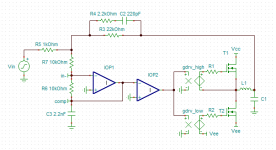
The IRS2092 is a bit of a strange contraption, it contains an OTA and a comparator, but doesn't give you access to all the required pins, this means a simple post-filter scheme like 1st order UcD is not simple to implement. I've tried a few things in the simulator, mostly a combination of pre- and post-filter feedback, which seems to work, but doesn't really impress at this point (no real benefits)
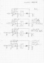
From reading some of the datasheet and chip brochures it appears that Jun Honda (IRF's designer for the IRS series) does hint at the possibility (http://www.irf.com/technical-info/whitepaper/499bps0802.pdf). I however have yet to figure out how to accomplish this with results that look promising. Something like this (http://www.diyaudio.com/forums/class-d/120100-irs2092-customizable-5.html#post3912755) could possibly work, but doesn't show promise in the simulator? See attachments for principle schematic.
- CSD:
You're right, the 100nF was an oversight, I was meaning to add some ceramics to the sensitive supply pins on the IC, but CSD obviously isn't one of them.
- Buffered gate drive:
Thanks for the insight, I hadn't thought about using one resistor per PNP/NPN that certainly looks to be a good way to control individual on/off. As for the PCB, it'll be 4-layer SMD for the most part. I plan on going with the IRFB4615 design for now, so I will not be requiring the totem pole buffers, unless you strongly disagree.
- Start-up of gate drive:
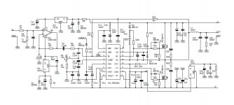
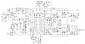
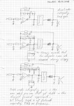
I'm assuming with VBS you mean VB, the high side driver supply? I've worked your suggestions into my schematic, could you please verify I've done this correctly? Parts added are R20 and D8 in the below noted schematic.
In the meantime I've also changed the front-end somewhat, I put in an inverting amplifier as I would like a non-inverting character for the whole amplifier. Input impedance is ~10K and the gain of the front-end is set to ~5x with the class-D section offering 4x gain, for a total of ~20x or ~26dB.
I've also implemented some housekeeping, the VCC (12V) supply, can now be turned on/off by T1. Which will go hand in hand with the 'ENABLE' pin on the IRS2092. The VCC supply will come up first with the CSD pin following ~2 seconds later. I plan on using either small PIC microcontroller (16F or 18F series) or logic gates (4093) for setting up the required IF/OR/AND/ELSE states needed.
As for housekeeping, how does one guarantee silent turn on/off? Is a power up sequence where VAA and VSS are always present but VCC (12V) is delayed enough for turn on? And vice versa for turn-off (i.e. VCC turns off first)?
Thanks so much for the informative post, so sorry to hear about the initial post getting lost in the digital abyss, I wholeheartedly agree with you that in this day and age this shouldn't happen.
Let me tackle your suggestions one by one and provide feedback:
- Input op-amp:
For the power rails I was looking to get better regulation than with just two zeners and some caps. Two SOT23 or TO92 regulators would suffice here, hence in terms of cost and complexity it doesn't add much. I realize the LME opamp's PSRR is stellar at >120dB, but I can't bring myself to run it off of power rails that are not properly regulated.
As for the differential input, I agree. This will be a 'plate amplifier' mounted on the back of the loudspeaker, hence it'll take the input off of the speaker terminals. I am planning on making the input section of the filter with a instrumentation amplifier, but after that, i.e. the Linkwitz transform, the active crossover, etc. the circuit will be single-ended.
- IRS2092 supplies and UVLO:
I'll use two SOT23 5V LDOs instead, if needed with an enable pin so I can turn the supply rails off before the squeals of death resonate from the loudspeaker. This ties in with the housekeeping comments at the bottom of this post.
- Post-filter feedback:
The IRS2092 is a bit of a strange contraption, it contains an OTA and a comparator, but doesn't give you access to all the required pins, this means a simple post-filter scheme like 1st order UcD is not simple to implement. I've tried a few things in the simulator, mostly a combination of pre- and post-filter feedback, which seems to work, but doesn't really impress at this point (no real benefits)
From reading some of the datasheet and chip brochures it appears that Jun Honda (IRF's designer for the IRS series) does hint at the possibility (http://www.irf.com/technical-info/whitepaper/499bps0802.pdf). I however have yet to figure out how to accomplish this with results that look promising. Something like this (http://www.diyaudio.com/forums/class-d/120100-irs2092-customizable-5.html#post3912755) could possibly work, but doesn't show promise in the simulator? See attachments for principle schematic.
- CSD:
You're right, the 100nF was an oversight, I was meaning to add some ceramics to the sensitive supply pins on the IC, but CSD obviously isn't one of them.
- Buffered gate drive:
Thanks for the insight, I hadn't thought about using one resistor per PNP/NPN that certainly looks to be a good way to control individual on/off. As for the PCB, it'll be 4-layer SMD for the most part. I plan on going with the IRFB4615 design for now, so I will not be requiring the totem pole buffers, unless you strongly disagree.
- Start-up of gate drive:
I'm assuming with VBS you mean VB, the high side driver supply? I've worked your suggestions into my schematic, could you please verify I've done this correctly? Parts added are R20 and D8 in the below noted schematic.
In the meantime I've also changed the front-end somewhat, I put in an inverting amplifier as I would like a non-inverting character for the whole amplifier. Input impedance is ~10K and the gain of the front-end is set to ~5x with the class-D section offering 4x gain, for a total of ~20x or ~26dB.
I've also implemented some housekeeping, the VCC (12V) supply, can now be turned on/off by T1. Which will go hand in hand with the 'ENABLE' pin on the IRS2092. The VCC supply will come up first with the CSD pin following ~2 seconds later. I plan on using either small PIC microcontroller (16F or 18F series) or logic gates (4093) for setting up the required IF/OR/AND/ELSE states needed.
As for housekeeping, how does one guarantee silent turn on/off? Is a power up sequence where VAA and VSS are always present but VCC (12V) is delayed enough for turn on? And vice versa for turn-off (i.e. VCC turns off first)?
Attachments
... Ensure stable VAA and VSS until the point the UVLO of the driver supplies will turn OFF the MosFets. In my measurements stable VAA and VSS also were helpful for perfomance.
In your schematic you are connecting D4 just somewhere to the rail.
In the layout you should make sure to connect it close to the drain of the high side MosFet. Otherwise the high side overcurrent protection may start phantom tripping due to noise.
Thanks, I've worked these changes into the schematic, please see post #76.
Eva,
Thank you for taking the time to provide such detailed explanations and information on this subject!!
In your opinion what manufacturers use the best implementation of this design type? Carvin, Berhinger and others provide have commercially available amps that are hard to beat for value. And of course the large selection of modules from around the world.
Thanks again!!
Scott
- Post-filter feedback:
The IRS2092 is a bit of a strange contraption, it contains an OTA and a comparator, but doesn't give you access to all the required pins, this means a simple post-filter scheme like 1st order UcD is not simple to implement. I've tried a few things in the simulator, mostly a combination of pre- and post-filter feedback, which seems to work, but doesn't really impress at this point (no real benefits)
Attached a simple evolution of possible post filter feedback arrangements.
The cap with the dotted line is not generally required, but can be helpful to stabilize when squeezing loop gain.
Start in simulation with the basic version. Feel free to get some starting point for values from ...well you know where.. 😱
After basic version runs, you can let it grow through the evolution.
The OTA with the need of 1nF to GND like in the IRS2092 is not the only way.
Basically a fast OP amp would be possible as well, but I think IR has chosen the OTA, because you can get a cheap OTA by building an OPamp but skip everything behind the VAS...
Edit:
Regarding clamping of the integrating gain:
It can be a simple clamp with diodes, or slightly more sophisticated with two BJTs, or an additional nonlinear local feedback like implemented in the very nice Kemp design.
Attachments
Last edited:
- Status
- Not open for further replies.
- Home
- Amplifiers
- Class D
- Tips and suggestions on IRS2092 implementation?