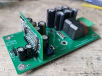
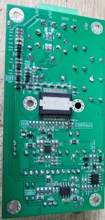
Tested the boards with a chip change to the TAS5162.
In BTL stereo version there is power increase only at 8ohm - 130W RMS, (135W@4Ohm OCP)
In the PBTL variant it was possible to 250W@4ohm. No-load consumption in this variant is about 8W
In BTL stereo version there is power increase only at 8ohm - 130W RMS, (135W@4Ohm OCP)
In the PBTL variant it was possible to 250W@4ohm. No-load consumption in this variant is about 8W
I need to ask this question because it appears to be unexplored.
Why does the amplifier have an adjustable frequency? In my recent simulations, I observed that randomly sweeping frequencies—or in your case, toggling between two frequencies—significantly influences the "system's overall transfer response" control theory domain. By selecting an "idle target frequency" and designing the poles and zeros around this point for different operational states, the "final set point idle frequency" is established. However, this necessitates readjusting the LC double pole at the output. Given these complexities, I'm curious why these frequency sweeps are conducted as a production "user settable" option, as they seem to complicate the predicted behavior of the control loop.
Why does the amplifier have an adjustable frequency? In my recent simulations, I observed that randomly sweeping frequencies—or in your case, toggling between two frequencies—significantly influences the "system's overall transfer response" control theory domain. By selecting an "idle target frequency" and designing the poles and zeros around this point for different operational states, the "final set point idle frequency" is established. However, this necessitates readjusting the LC double pole at the output. Given these complexities, I'm curious why these frequency sweeps are conducted as a production "user settable" option, as they seem to complicate the predicted behavior of the control loop.
In this case, I didn't notice an impact in the audio range.
The frequency boost option activates the feedback before the filter, as it is realized in the original ET400 modules.
But since the delay in my circuit is much lower than in the ET 400, even without the additional boosting OS, the frequency is 600-640kHz
The frequency boost option activates the feedback before the filter, as it is realized in the original ET400 modules.
But since the delay in my circuit is much lower than in the ET 400, even without the additional boosting OS, the frequency is 600-640kHz
Interesting, I think the influence of the loop are during "modes" and NOT audiophile listening evaluation.
I read the paper and noticed some areas of interest like clip recovery and current trip under operations such as loud playback or even shorting the output.
- 600-640kHz I cannot seem to get an IRS20957 (due an already internal 350ns delay + 10ns comp delay) using an NCORE modulator to go that high, not without 100p/220p lead/lag networks, I don't like 10^-9 pico farad values in loops they seem to be sensitive to finger touching drift.
Thanks for the correction, I would like to explore and hear more about behavior analysis in the future I noticed the question wasn't answered for now.
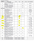
Sorry I had some doubts on the figure you supplied, where did you get 140ns? I had a look at the datasheet for the IRS20957 and here are the exact figures.IRS20957 latency is about 140ns with switches and comparator.
Updated for Minimum, Typical and Maximum.
Minimum Delay Calculation:
- Turn-on rise time (tr): 15 ns
- Turn-off fall time (tf): 10 ns
- Turn-on propagation delay (Ton1): 95 ns
- Turn-off propagation delay (Toff1): 80 ns
- Minimum deadtime (DT1_min): 8 ns
tp1_min = Ton1 + tr + DT1_min + Toff1 + tf
tp1_min = 95 ns + 15 ns + 8 ns + 80 ns + 10 ns = 208 ns
For non-floating inputs:
tp2_min = Ton2 + tr + DT1_min + Toff2 + tf
tp2_min = 95 ns + 15 ns + 8 ns + 80 ns + 10 ns = 208 ns
Typical Delay Calculation
- - Turn-on rise time (tr): 15 ns
- - Turn-off fall time (tf): 10 ns
- - Turn-on propagation delay (Ton1): 95 ns
- - Turn-off propagation delay (Toff1): 80 ns
- - Typical deadtime (DT1_typ): 15 ns
For floating inputs:
tp1_typ = Ton1 + tr + DT1_typ + Toff1 + tf
tp1_typ = 95 ns + 15 ns + 15 ns + 80 ns + 10 ns = 215 ns
For non-floating inputs:
tp2_typ = Ton2 + tr + DT1_typ + Toff2 + tf
tp2_typ = 95 ns + 15 ns + 15 ns + 80 ns + 10 ns = 215 ns
Maximum Delay Calculation:
- Turn-on rise time (tr): 15 ns
- Turn-off fall time (tf): 10 ns
- Turn-on propagation delay (Ton1): 95 ns
- Turn-off propagation delay (Toff1): 80 ns
- Maximum deadtime (DT1_max): 22 ns
For floating inputs:
tp1_max = Ton1 + tr + DT1_max + Toff1 + tf
tp1_max = 95 ns + 15 ns + 22 ns + 80 ns + 10 ns = 222 ns
For non-floating inputs:
tp2_max = Ton2 + tr + DT1_max + Toff2 + tf
tp2_max = 95 ns + 15 ns + 22 ns + 80 ns + 10 ns = 222 ns
Total Minimum Delay: 208 ns
Total Typical Delay: 215 ns
Total Maximum Delay: 222 ns
Attachments
Last edited:
I propose that you take measurements on the prototype 😉
For intrigue, the output stage on the TAS5342 has an input- to power output delay of 43ns.
For intrigue, the output stage on the TAS5342 has an input- to power output delay of 43ns.
Hi sous can I ask you for a huge favor please, could you post a measurement from one of your kits using the IRS20957 and show the scope delta measurement of the IC delay as you seem confident, its not that I don't trust you, I'm curious is this data a result of a part sourced from china that differs from the datasheet.
sorry if the thread is going off the point of the TAS5342 work you which is pretty impressive, might I say.
sorry if the thread is going off the point of the TAS5342 work you which is pretty impressive, might I say.
I have a prototype on chip YD7127 (copy of IRS20955).
Reference point on the PWM input, voltage transition through the level of 2V.
Delay of 152ns until the signal at the half-bridge midpoint passes through zero.
I.e. the delays in the chip and output transistors are taken into account here. YD7127 is also slower than IRS20957.
Reference point on the PWM input, voltage transition through the level of 2V.
Delay of 152ns until the signal at the half-bridge midpoint passes through zero.
I.e. the delays in the chip and output transistors are taken into account here. YD7127 is also slower than IRS20957.
Any chance you could upload scope pictures with the measurement ?
Also you don't own anything with genuine IRS20957 parts for figures?
Also you don't own anything with genuine IRS20957 parts for figures?
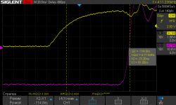

IRS20957= Yellow Trace, Purple=IRFB5615 VdsIRS20957+IRFB5615
Is this an original IRS20957? or IRS20957 (YD7127 clone) @ 114ns delay
yes, origin 20957
my amp module 2_061, yellow - PWM, purple D-S (inductor)
purple without gnd connection
PS Yes, there's also an additional transistor stage at the output of the 20957 on the complementary pair ss8550/ss8050 also adds a few nanoseconds.
my amp module 2_061, yellow - PWM, purple D-S (inductor)
purple without gnd connection
PS Yes, there's also an additional transistor stage at the output of the 20957 on the complementary pair ss8550/ss8050 also adds a few nanoseconds.
Last edited:

- Home
- Vendor's Bazaar
- TI power stage for selfoscillating amplifier