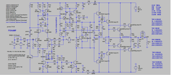


Move D8 to the collector Q1. This will keep the collector voltages on Q14 and Q15 the same. This will help keep the current mirrors matched thermally as vbe changes with temperature.
Jeremy
Jeremy
Lower R9 and R34 to 24kohms. This will bump the current up on the Red LEDs to about 1.5mA.
Jeremy
Jeremy
Same difference. It doesn't matter if D8 is on the emitter or collector, clip recovery will be the same. During the posistive half cycle clipping D3, D8, and Q1(when saturated) form a Baker Clamp around Q30.Does it recover from clipping?
Jeremy
It was meant as a question to LKA, but anyway, does "the same" mean that both circuits end up in a huge limit cycle from which they never recover or that they both work fine after clipping?
The reason I'm asking is that loops with an order greater than two have the reputation of bursting into oscillations after clipping or start up. That reputation is not entirely deserved, as some work just fine, while some circuits with simple, low-order compensation schemes do burst into oscillations.
The reason I'm asking is that loops with an order greater than two have the reputation of bursting into oscillations after clipping or start up. That reputation is not entirely deserved, as some work just fine, while some circuits with simple, low-order compensation schemes do burst into oscillations.
Last edited:
Clipping behavior will act the same and will perform very well. This part of the circuit has been copied from the Wolverine of which I helped design.
Jeremy
Jeremy
wow ! (CK1-3) (R71/C18) ... lead and lag ? (C4/R4 - C3/R3). That be a lot of (complex) compensation. Break out the tian probes !
I apologize...
Q39, Q40, Q41 can be BC546/BC556. They're 65V parts which are adequate for your rail voltages. I was mixing them up with BC550/BC560 which are 45V.
Anyways, this looks like a interesting compensation idea.
Jeremy
Q39, Q40, Q41 can be BC546/BC556. They're 65V parts which are adequate for your rail voltages. I was mixing them up with BC550/BC560 which are 45V.
Anyways, this looks like a interesting compensation idea.
Jeremy
I'm a big fan of LKA's design. Below is a link to an earlier project:
https://www.diyaudio.com/community/...ee-pole-compensated-class-b-retro-amp.385080/
https://www.diyaudio.com/community/...ee-pole-compensated-class-b-retro-amp.385080/
H
HAYK
Nyquist's stability criterion. It's been known for about a century that feedback loops with more than 360 degrees of phase shift around the loop at frequencies where the magnitude of the loop gain exceeds unity can be stable, as long as the phase shift returns to smaller values before the magnitude of the loop gain becomes unity.
See post #9 of https://www.diyaudio.com/community/...n-loop-gain-of-1-000-000-000-000-000-p.16936/ for a simple demonstration circuit.
See post #9 of https://www.diyaudio.com/community/...n-loop-gain-of-1-000-000-000-000-000-p.16936/ for a simple demonstration circuit.
Last edited:
It used to be impopular in the valve age, because valve amplifiers with such compensation usually oscillated when the cathodes were not fully heated up yet. Since the 1990's, it's been used all over the place in sigma-delta audio DACs and class-D amplifiers. Only class A, AB and B amplifier designers keep holding on to order <= 2 compensation schemes - except LKA.
Hi LKA,
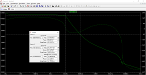
How much loopgain is that at 20kHz? Looks like >60dB with predrivers included. That loopgain plot looks pretty nifty. I gotta try that 3 pole stuff.
What function are D8 & D3 serving? Clean clipping perhaps?
I suggest driving Q41 from the output. This will likely yield better CMRR as it did with my designs.
Cheerios,
Ruben
Has anyone noticed that IPS/VAS is almost an exact copy of wolverine, only upside down ? Including lead-lag compensation, etc
ULGF 3 MHz
PM 65 deg
GM 18 dB
LG1k 113 dB
LG10k 110 dB
LG20k 88 dB
the power supply voltage is +-48V at idle , so with real components it will give 170W/4R
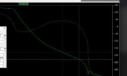
The images below capture the simulation into 4R
20k clipping
10k 80Vpp square wave
ULGF 3 MHz
PM 65 deg
GM 18 dB
LG1k 113 dB
LG10k 110 dB
LG20k 88 dB
the power supply voltage is +-48V at idle , so with real components it will give 170W/4R
The images below capture the simulation into 4R
20k clipping
10k 80Vpp square wave
Attachments


Last edited:

"Move D8 to the collector Q1. This will keep the collector voltages on Q14 and Q15 the same. This will help keep the current mirrors matched thermally as vbe changes with temperature."
On the schematic IPS Wolverine, D9 is also in the emitter of Q12.
Does the diode position (emitter vs collector) mean a lot ?
"Lower R9 and R34 to 24kohms"
thanks, I missed this
On the schematic IPS Wolverine, D9 is also in the emitter of Q12.
Does the diode position (emitter vs collector) mean a lot ?
"Lower R9 and R34 to 24kohms"
thanks, I missed this
- Home
- Amplifiers
- Solid State
- Three-pole compensated blameless clone