You mean I have to include the modulator gain also by putting the voltage source between comparator and error
amplifier?
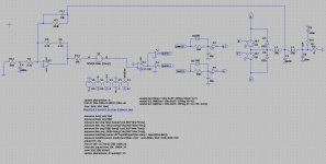
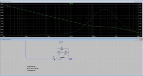
Not quite. Your switching model includes it as of right but if you tried to implement a linear model such as,
Here the gate, Modulator, has been replaced by a Voltage Controlled Voltage source with a gain set to the nominal Vhigh=2.5 Vlow=-2.5 of the gate including a delay element in the cunning expectation, hope, of getting a 'correct' result for loop gain in the linear representation.
The loop crossover frequency is higher than with the, real, switching model because the real modulator gain has not been properly accounted for.
The argument, and I have not got my head around reality as yet so the following might not be totally correct. You might start out by looking at things in terms of a triangle wave based modulator.
As MODIP traverses from -0.5V to +0.5V MODOP, filtered, traverses from -50V to +50V. The modulator gain is 100.
Move both inputs to the same input on the comparator.
The result is the same with a modulator gain of 100.
In the self oscillating case you might consider two paths through your loop. One for the low frequency, audio, signals and one for the high frequency, switching signal(s). The high frequency one will be the self-oscillating frequency modified by the loop.
At a simple level the modulator gain becomes some function of VLF/VHF with VHF being equivalent to your triangle wave which is kind of where my reasoning falls over or rather, for the moment, I can't quite follow things through. The above could be a reasonable implementation but beyond that in the self-oscillating case VLF and VHF appear in the same path. Take a leap of faith and.
Which would be equivalent to.
I'm not sure if the above helps your, or my, understanding. Perhaps you were already there.
Attachments
Oke, I see I have done not right now, because I do not use a triangle, who gain is supply voltage divided by
two divided by triangle voltage. what will then 80 x.
I try again with output to error amp as before.
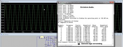
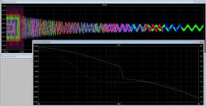
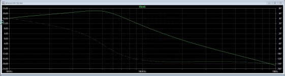
Done in 12 minutes. See that I have not that much gain, for proper correction we need a least 60dB, yes for this the simulation
is quite usefull.
Now a little a roller coaster gain plot. But nice to play with and learn some, as is Spice for me a little to much, real time build
is the best. I did find in the designs also a current feedbacked version, nice to try.
however sometimes I have two feedback, post and pré and now question arrives how to use feedback then in spice. because
I have two path and one source.
I go read that article some times to see.
Thanks for all the help. appropriate it,.
two divided by triangle voltage. what will then 80 x.
I try again with output to error amp as before.
Done in 12 minutes. See that I have not that much gain, for proper correction we need a least 60dB, yes for this the simulation
is quite usefull.
Now a little a roller coaster gain plot. But nice to play with and learn some, as is Spice for me a little to much, real time build
is the best. I did find in the designs also a current feedbacked version, nice to try.
however sometimes I have two feedback, post and pré and now question arrives how to use feedback then in spice. because
I have two path and one source.
I go read that article some times to see.
Thanks for all the help. appropriate it,.
Attachments
Oke, I see I have done not right now, because I do not use a triangle, who gain is supply voltage divided by
two divided by triangle voltage. what will then 80 x.
No... You're racing ahead of things, again, or I'm not explaining very well. I used a triangle wave in order to develop an idea. There is no triangle wave in a self oscillating amplifier. It is replaced by the switching frequency as it appears at the input to the modulator. I'll try to develop the idea or make more sense in my next post.
For the moment you are doing it right.
I do now, I did explain this wrong. your idea was for explain me.
I did write it some confusing way.
I
I did write it some confusing way.
I
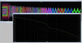
I have extent the loop, see that fase is affected following now th gain plot. This
did stay the same, looks closed loop, but did affect the fase.
The other pic is how it needs to be, a 60 dB open loop gain, the gain is constant
over audio pad and I did use the flattened integrator for this.
did stay the same, looks closed loop, but did affect the fase.
The other pic is how it needs to be, a 60 dB open loop gain, the gain is constant
over audio pad and I did use the flattened integrator for this.
Attachments
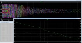
Did you remember I did say that the feedback of the amp earlier that it did
also oscillate in the Mhz range and on the normal 400 Khz range as needed?
So I have two carriers and unstable system,.
Now I see why, so this is quite useful. Get a drop below zero dB as needed but it get gain again.
I can not see what happens above 1 Mhz, but this looks not very stable.
This plot is a other feedback, I have more, so play with it, nice stuff. But I have also use
the post feedback and not the pre feedback who is also there, this I have not yet clear.
Attachments
Now I see why, so this is quite useful. Get a drop below zero dB as needed but it get gain again.
I can not see what happens above 1 Mhz, but this looks not very stable.
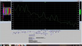
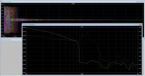
It is not useful because the plot is garbage containing little to no meaningful information. The nature of the analysis is such that it is at best subject to noise and at worst, should your system be unstable for some reason at one of the stepped frequencies or the analysis starts with an incorrect operating point, does not give a valid answer. That results in the spikes from one data point to the next in your plot.
The fact that you want to believe the results just adds to my general view that you do not understand or want to understand what is going on in these circuits. You are literally just throwing in other people's kitchen sinks and fiddling for effect.
These things can be go, no-go or go somewhere else. There may be a solution, your desired one, where self oscillation occurs at 500KHz but there may also be another solution, one you did not expect, where self oscillation occurs at 10MHz that for a particular set of circumstances or conditions is the one the simulation flips into.
That it is garbage I did see but simulation and read this is for me difficult. I had success the normal way also, by calculations
and then sim it, the ac performance of the lead/lag compensator I did with ac sims.
I keep it on the normal as I did, I think that is better then stuff I do understand not properly..
Just calculate and sim open loop I can see what is needed and build real time it the proper way to go.
I have already stuff done to go build a front end an go there. I see not that using such plots do work for me.
Need open loop to be high, I did use cascade flattened integrator s with forward resistors and get quite good results, I can see
it on sim with just a ac plot. then use it in real time after complete a circuit.
The double oscillation I have not with your models here, It was because I had put poles very high and zero low. For audio there is
the need for a proper bandwidth, even extent it beyond low pass. I did read a lot of stuff, and all come to the same conclusion, it is
difficult to get a good sounding class D, the ice-power does but sounds flat. I saw patents, but all is does look quite the same, cascaded
delta sigma looks do well, but low pas including needs work.
the circlotron with auto-bias is U think better, but class d did interest me, but have not so much experience with.
Gan mosfets however will upgrade class d.
and ?
Did you hear probably from someone else here. I am 65 I do not so fast put things into mine brain anymore. I do not steal stuff, it just
electronics, and already mucho mucho repeated circuits with just minor changes in patents. Class D is maybe still fresh here.
thanks for help.
and then sim it, the ac performance of the lead/lag compensator I did with ac sims.
I keep it on the normal as I did, I think that is better then stuff I do understand not properly..
Just calculate and sim open loop I can see what is needed and build real time it the proper way to go.
I have already stuff done to go build a front end an go there. I see not that using such plots do work for me.
Need open loop to be high, I did use cascade flattened integrator s with forward resistors and get quite good results, I can see
it on sim with just a ac plot. then use it in real time after complete a circuit.
The double oscillation I have not with your models here, It was because I had put poles very high and zero low. For audio there is
the need for a proper bandwidth, even extent it beyond low pass. I did read a lot of stuff, and all come to the same conclusion, it is
difficult to get a good sounding class D, the ice-power does but sounds flat. I saw patents, but all is does look quite the same, cascaded
delta sigma looks do well, but low pas including needs work.
the circlotron with auto-bias is U think better, but class d did interest me, but have not so much experience with.
Gan mosfets however will upgrade class d.
and ?
literally just throwing in other people's kitchen sinks and fiddling for effect.
Did you hear probably from someone else here. I am 65 I do not so fast put things into mine brain anymore. I do not steal stuff, it just
electronics, and already mucho mucho repeated circuits with just minor changes in patents. Class D is maybe still fresh here.
thanks for help.
Attachments
Last edited:
Perhaps I am on the verge of destroying a friendship that I didn't really care about in the first place by using the wrong words <- Look I've done it again.
It's not entirely intentional.
Note to self, you can ignore this one. Blagging other people's stuff is not stealing. However blathering about other people's stuff is just silly.
My problem here is that I am only 59 but you are 65 and have done things I don't, as yet, understand.
I don't understand it because I am trying to come to terms with what might be going on and you are racing off with 5th order blah blah PID hypergolic rocket engines and can't, realistically, explain them.
If I could be bothered I would try to explain the following, where I am at the moment, but you are well ahead of the curve on such matters so you you can tell me why this works assuming you care to bother looking at the pictures.
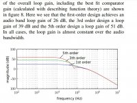
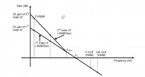
Target self oscillation frequency is 500KHz. Your hint would be the filter has a cutoff at 50KHz. DC loop gain is 0.01. Second order filters go -40dB per decade. Add some, meaningful, poles and zeroes.


And No. I do not care about your latest nth order multi feedback hell circuit or how you do not really know why it might improve the performance of the above.
Hate you later.
Night Night.
It's not entirely intentional.
Note to self, you can ignore this one. Blagging other people's stuff is not stealing. However blathering about other people's stuff is just silly.
My problem here is that I am only 59 but you are 65 and have done things I don't, as yet, understand.
I don't understand it because I am trying to come to terms with what might be going on and you are racing off with 5th order blah blah PID hypergolic rocket engines and can't, realistically, explain them.
If I could be bothered I would try to explain the following, where I am at the moment, but you are well ahead of the curve on such matters so you you can tell me why this works assuming you care to bother looking at the pictures.
Target self oscillation frequency is 500KHz. Your hint would be the filter has a cutoff at 50KHz. DC loop gain is 0.01. Second order filters go -40dB per decade. Add some, meaningful, poles and zeroes.
And No. I do not care about your latest nth order multi feedback hell circuit or how you do not really know why it might improve the performance of the above.
Hate you later.
Night Night.
Attachments
Last edited:
Maybe I am not quite wake-up, I have a friend with breast cancer and is metastasized to liver and lungs. This is not
a joke and not a way to talk myself out of it.
I never do not destroy friendships because I am not understand something, that is such a bad habit, you do just tell the truth,
I am not that good with LTspice. I will accept that without problems.
You have extensively knowledge about LTspice and can put a simple circuit into it what works, I can also but use then models
like a gate driver, that do slow down unfortunately. but have also use fast models also now that makes things more easy. But I have
now seen your setup, and it looks like I have done some errors also, I have for example used not a input signal source. I did not read enough
about this way of simulation of gain so I go read extensively now. I did always sim with AC the open loop response, it does work for that,.
I did play with poles and zero,s in some circuits, and use triangles, multilevel etc. you have done also making response better. As I say I go read that article for sim gain better, I did see it was wrong on mine side. in pics you have done that with one op amp. I think with Gan mosfets who are now the future,, playing with old mosfets and extensive feedback can be dramatically eased, no body diode, faster switching, but strong rules on pcb design as after sale to get dt not damage the Gan, then we need not such big poles and zero,s to error correct switching. But these Gan are small and sensitive, needs a whole new approach to use them.
On pic,s I have plot from a paper, and the resulting circuit with two op amps, you did this with one. Nice less op amps the better, but gain will change.
Did you hear ever about flattened audio band in integrator of error amp? with resistor over small cap so audio is outside integrator. and gain get constant,
over whole audio band. And not forget lag lead correction for post feedback, here things get difficult with class D, except maybe when use multilevel or Gan on high freq carrier. I did include a pic, where you can see the low pass and the lead/lag correction, nice mirror. I did simulation with AC in spice open loop to get that response.
One of your has a AC simulation, this I do all the time, but including a pwm is what I think is not that good there, I did use just a gain block here for closed loop response. I see also that your circuit is LTspice on his best and here I get into trouble.
I go look deeper into this to have some more pleasure playing with it. Class d on it's own is not complicated time domain stuff, but get it right, linear as possible and stable is.
But thanks for hating me.
appreciate your help of course,
Attachments

And No. I do not care about your latest nth order multi feedback hell circuit or how you do not really know why it might improve the performance of the above.
Hate you later.
I never say it is better, I was already for simple system with highest quality. I have read a lot of papers to get some info about class D
much is already done, so not all, and newer idea,s less born.
We also need to think that it will go full digital in near future. Also here is a lot work done, but Gan will help.
In fact it are quite good transmitters. do it drop in carrier, it get a buck and burn your speakers.
So carrier based are much more save, and also easier to design feedback, however other things happen, like
clock jitter.
Maybe a smart idea of a single op amp 4th order filter does spare a lot parts like op amps, that is what I also like,
the neat Phillips UCD is a nice thing. Sound of Phillips was always good, but I have still a own build mosfet hybrid
where tubes are dc coupled to mosfets with a dc servo and auto-bias, already play for 15 years now, never failed
but also never build in case, still just a wires and wires spaghetti.
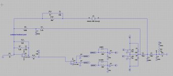
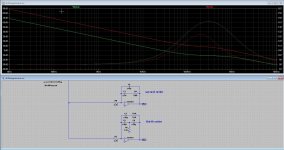
Oke that said, you have send some sim files and I did look at that, I see you have feedback voltage source A and B
between error amp and modulator the comparator. I did ask last if this has to be done, because now it looks like
I get better results, I have now used a current/voltage feedback circuit I did drawn some years ago. But your sim
files did help a lot to understand some more about the ltspice, still, I am greener then green behind the ears what
concerns LTspice programming side or how that is called..
As last, I have now again did what you have said, after some more reading in it and look at your circuit, have
use mine circuit and put it in like in yours. So I get a much better picture of the idea.
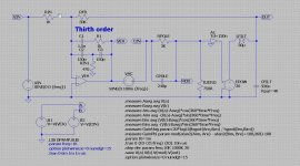
In pic also a single opamp thirth order error amp, I like more then cascaded mucho opamps.
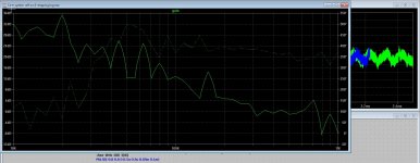
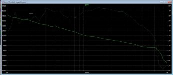
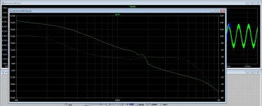
The plots are from the voltage/current feed-backed circuit I draw a time ago for testing that, I see in the plot it
does a abrupt fall off at 0 dB on 800Khz, cause more noise to output.
Fase looks quite good, no dangerous things. But that 800 Khz where it go real down is bad for noise, and that
is also present in plots.
Looks it is usefull plots, but can be wrong, witch I aunt.
regards
Attachments
So before I go drink the beer and go to sleep.
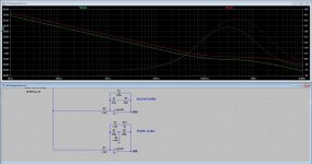
I have done some play with your circuit I do go to see it's intentions.
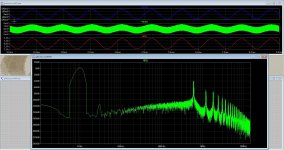
Now I know what LTspice plot does much more, but see here that this is quite useful to optimize the gain
all is visible. On the left of the plot I see the noise what is left after the higher frequency's get suppressed, also
here find the best spot. But that I did also now because it is part of the designing.
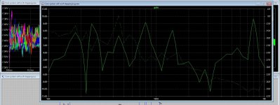
in pic you see that changing the parts has a impact on the gain, fo from 54 dB to 40dB but looks cleaner. so I go play some more and hope I can be friends again (joke)😗.
I have done some play with your circuit I do go to see it's intentions.
Now I know what LTspice plot does much more, but see here that this is quite useful to optimize the gain
all is visible. On the left of the plot I see the noise what is left after the higher frequency's get suppressed, also
here find the best spot. But that I did also now because it is part of the designing.
in pic you see that changing the parts has a impact on the gain, fo from 54 dB to 40dB but looks cleaner. so I go play some more and hope I can be friends again (joke)😗.
Attachments
Hi There
Did some play with this ltspice model, and it is useful in some way, I can see what result it has.
I do open loop sim and the response of the feedback opamp and the pid around it with AC simulation.
Noise stuff, for this the sim has the most value because I can see the response and where the 0 dB point is.
in most designs who look all to each other. But in near future and with gan I think it will go total digital
getting a power dac who works fine.
Here some play with model to get comfortable with it.
Attachments

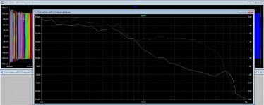
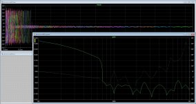
On AC I get also useful info, the open loop response. As you see it runs out of steam higher in
frequency, that makes that the distortion rise on higher frequency's.
That is why cascaded is used, with flattened audio band and forward resistors give better
results, but say not much about quality of audio, as we all now extensively feedback does not
more good flattening audio quality. Pic 2 (red line) is such a system, you see 90dB loopgain with a
thirth order and one op amp, but when I change the lead phase to a higher value the gain drops. as
seen in pic 3. I have the unity point on the frequency output filter and use the lead fase to correct
for stability and proper feedback special for higher frequency's etc etc,.
I build such amp to see in real time, the protections etc I do not have for now, that is easy stuff,
I do use dead-time, who is already in mosfet driver.
This is mine way to play and see what happens. This time domain stuff is quite interesting.
Attachments
Last edited:
Hi
Have included now the calculation from a paper who does lead/lag compensation and have formula,s who are good
understandable for me.
The stuff I have changed in your circuit and make a thirth order with one op amp, I like less op amps in audio systems.
I have calculate the lead to be on the low pass filter bandwidth, and it,s outcome is quite good, low noise, because the
unity point is low. it does change with carrier, but keeps at distance.
I do not now what you think, but for me this looks very good, special the deep notch around 0dB take care for low noise.
I go try you other circuits, I thought that I saw you did included there comparator. extra gain.
The plots are with different carriers, I did set delay higher because it was above 1 MHz that is why that plot do look some better.
I hope I get now the good entrance in it, special for the simulations, still, what you can here, I can not, but I read about it and
find always some info.
Attachments
Sorry to hear of your friend and apologies for my rant. You have raced ahead.
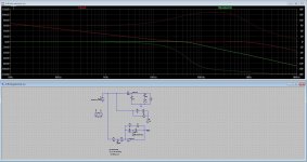
The point of my last post which I did not get around to and only realised later is that I have been trying to get things right in my head as to what determines the modulator gain. You may know this already but it was staring me in the face.
The linear model of the loop, my version.

It's response.

Being me and bored with it all I used CPVE to tip the phase over to 0 degrees at 500KHz which became the self oscillation frequency. You should be able to do the same for your weird and wonderful circuits in a similar linear model.
The in my face thing is that that zero degree point also defines the amplitude of the switching ripple frequency, -42dB, which defines the modulator gain, +42dB to arrive at 0dB at crossover so the curve in the linear model, probably not the full picture, just gets shifted up accordingly.
It is tempting to comment further on some of your plots but I shall once again shut up again for a bit.
The point of my last post which I did not get around to and only realised later is that I have been trying to get things right in my head as to what determines the modulator gain. You may know this already but it was staring me in the face.
The linear model of the loop, my version.
It's response.
Being me and bored with it all I used CPVE to tip the phase over to 0 degrees at 500KHz which became the self oscillation frequency. You should be able to do the same for your weird and wonderful circuits in a similar linear model.
The in my face thing is that that zero degree point also defines the amplitude of the switching ripple frequency, -42dB, which defines the modulator gain, +42dB to arrive at 0dB at crossover so the curve in the linear model, probably not the full picture, just gets shifted up accordingly.
It is tempting to comment further on some of your plots but I shall once again shut up again for a bit.
Weird and wonderful I like to hear. I do combine most of the time circuits, I have never had high school for it I am the time of the tubes,
but you also, but has properly a electronic profession. I was a shoemaker.
By the way a thirth order compensator is nothing strange, I like the simplicity, but some less gain. your plot is very clear for me, I did read 180 degree
does make a oscillator but here we need to see this some different because of the total delay etc. I have did make the delay in your circuit bigger because
I had 1.3 Mhz carrier frequency, changing the compensator was not the good idea, so did make delay higher...
Oke your are right about the plot needed to get down below 0dB to get less ripple, I get -18 or so and after some strange behavior, I see your is quite some more stable, mine plot has properly a very unstable oscillation. in pic I did yours with the thirth order compensator included, we have to now that we not only
need to get low ripple but also need of proper correction of the output filter and output stage, that is what makes it difficult.. class d is not that simple as analog, even if it is see as also a analog system operated in time domain .
I go look tomorrow, I did see your right here as you had all the time, I see now easily why I get 1 MHz carrier and low ripple where phase cross it, I can play with the zero and down it, result is lower gain and suppression get to -10 dB so more ripple, as you now and I see, it needs quite adjustments and these are minor. Oke, now I go further on this, getting more familiar with it. I have try in your circuit and ac sim, the thirth order does not that much except push oscillation into the MHz range, but then no -48dB but -20db.
Oke you have set the compensator to the cutoff frequency of the low pass filter for lead correction. on pic I did set delay back and use the zero of the lead compensator to set the frequency, I see it does match. Oke, now I now better the relationship. to set it such that phase get on the right place and low pass function compensator is on the right spot. But it does impact almost all, and compromises are needed. I have included also the ac plot with the thirth order compensator, it as the same plot but other gain. low pass on output is quite included and important where the cutoff is, but carrier will change with it make things even more difficult. One thing I do now for sure here, If it is Too Good To Be True, it mostly is.
What I still have to ask, I did look at phase where it was -90 (plus 90 integrator) or so for carrier frequency like in ice-power com system, but I did see by you it is where phase crosses the signal itself -20 or -200 or whatever is not to look at, but compensator does influence it also. and total delay system, this I did now.
Thanks for reaction and wishes for mine friend. And I am tough, just drill me military. because you are the master here not me, I do learn from it let me have something to do.
I am thankful for.
regards
Attachments
Last edited:
- Home
- Amplifiers
- Class D
- Three level flying cap Gan.