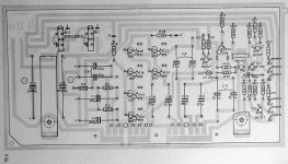
Could you please watch this picture.
Are the t1-t5 points are the same with the schema of the pcb one bridge version?
I removed t5 from this photo. I only used this for the transistors as I think numbers are the same. But I not sure fore t4-t5.
Are the t1-t5 points are the same with the schema of the pcb one bridge version?
I removed t5 from this photo. I only used this for the transistors as I think numbers are the same. But I not sure fore t4-t5.
Attachments
Last edited:
All these results aren't logical.
Are you certain you are getting a good connection with your meter on the various points. If there is any flux and varnish on the board then that can insulate the meter probe and cause incorrect readings.
The 'no voltage' on the base of T5 (when its removed) is an absolute. There is no route for any voltage except via leakage on the board, or a leaky C10 (but its not that).
Do you see 🙂 Nothing is making sense.
Could you please watch this picture.
Are the t1-t5 points are the same with the schema of the pcb one bridge version?
I removed t5 from this photo. I only used this for the transistors as I think numbers are the same. But I not sure fore t4-t5.
It is different in quite a few places, for example there is a 150 ohm resistor on the emitter of T3, R24 I keep mentioning is marked as R25 on this diagram. There is no C9 that I can see...
Could you please confir that t4 here is t4 there? Or t4 is t5 and t5 is t4? I couldn't understand it.
The layout of the transistors looks the same but there are several differences to the circuit details. Its obviously been modified in production.
So if t5 are the same I defenetly have 5V DC on the t5 base with the removed T5!!!
Last edited:
Yes, T5 is the same.
The 42k from the base of T5 that goes to ground is R25 on your board layout above. Yes, do you agree ? If you don't then say so 🙂
So one end of that resistor is grounded (so zero volts on that end), and the other end goes to the empty pad where the removed T5 was. So there should be zero volts on that end too (because resistors can't generate voltage).
Now the three caps, C11, C12 and C13 (all different numbers compared to the single bridge layout) on the above board feed onto the base of T5 via the switch (one cap at a time depending on switch position) but as caps do not pass DC current they can not be causing the voltage you see on the base of the removed transistor.
So you need to find why you read 5 volts on the base pad of the removed transistor. No component in the circuit can cause that.
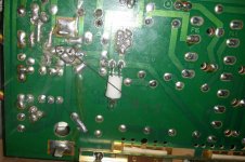
This is the photo of the t5 removed. I have 5-6V on this base (point on the bottom that is soldered). It connects to the resistor that is connected to the bulb
The bulb goes between T4 base and ground. The 42k resistor also goes to ground and so it can appear that the bulb goes to a resistor.
I'm out of time for today.
I really don't know where we go next because I can see you are really struggling with the component references and identifications.
If you really really do have 5 volts on the base of T5 with it removed then your problem is a physical short or leakage of some kind, perhaps within the switch... but the switch looks clean and good in the picture.
Should I throw this PCB away?=(
Nooo.
on the T5 base is REALLY REALLY 5-6V DC. Is it possible to trace where the voltage comes from?
And that is with T5 removed ?
Yes, its possible to trace where it comes from. One for tomorrow 🙂
It can't come from the 42k resistor. The path to check would be where the print goes into the switch. If the voltage is really there then something unwanted is feeding onto that piece of print.
Yes it's going to the switch on the bottom/ I have the same voltage here
As you see on the photo T5 is removed! I have 5-6V from T5 base to the ground of the transformer (green wire).
As you see on the photo T5 is removed! I have 5-6V from T5 base to the ground of the transformer (green wire).
Last edited:
Yes it's going to the switch on the bottom/ I have the same voltage here
So look at which contacts on the switch it is and which other contacts the switch connects together. Is there anything sticky on the board. Has it been cleaned with some weird cleaner that might be slightly conductive ?
If you can't find anything then is it possible to slip a piece of paper or plastic under that contact to isolate it and see if the voltage goes away.
Be creative in how you look for it... think outside the box 🙂
- Status
- Not open for further replies.
- Home
- Source & Line
- Analogue Source
- Thorens 125 MK1. Help me please repair this PCB.