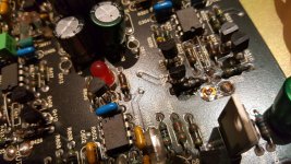
I picked up a Theta Gen Va DAC today and once I turned it on it failed on the left analog output stage. I pulled the plug and opened it up and noticed Q309 (MPS8099) has failed & adjacent resistor R325 burned up (+ Side of Differential Left Output). I also noticed R426 (still measures 10 ohms lol ) which is associated with the - (Negative) Side also burned up & the associated transistor Q410 (MPS8099) looks physically good but measures off spec.
Is there anyone familiar with the output stage of the Gen V/Va or has a schematic and/or can give me a hand understanding the analog circuit.
Any help would be appreciated.
Thanks in advance,
Is there anyone familiar with the output stage of the Gen V/Va or has a schematic and/or can give me a hand understanding the analog circuit.
Any help would be appreciated.
Thanks in advance,
Attachments
Last edited:
Someone plugged in a fast IC
The in-series coil was also removed -> bridged-out (to "improve" the sound)
The IC was oscillating wildly while the transistors were open (stop mode), large hi freq current ran from Vcc/Vee, through the IC's and then through the second muting transistors CE, and the resistor, to the ground, resulting in burnt-out components. This is at least what I think had happened... a MOD gone wrong...???
Just replace the IC's, use 100-ohm resistors instead of the coils that were removed, and replace the muting transistors/resistors. Transistors could be any... (you could even use a single Darlington type with a bit of re-wiring underneath...)
If you remove the socketed IC's, burnt transistors and resistors, you will be able to confirm the Vcc/Vee
If you just replace the IC's and install the 100-ohm resistors in place of coils, the thing will work even without shorting (muting) transistors/resistors - the muting circuit can be added later, once you start hearing the sound again
Last edited:
Analog Stage Schematic or Sketch Request
Thanks for your response but the Opamp in question (AD707) is a ultralow drift (with a slow 0.3V/usec slew rate) type that was standard in the Gen V.
I believe the removal of the inductor was an upgrade by Theta for the Version A of the Gen V version along with tightly matched 24 pairs MPS8099/8599 bipolar transistors (versus loosely matching these in the earlier Gen V).
I believe Theta biases these transistors heavily into Class A and as a result a lot of heat is generated and reliability is affected.
SO I want to understand the design of the analog stage versus trying to draw it out, so I was requesting if anyone has the analog stage schematic or has drawn it out as part of a troubleshooting exercise.
Any further help would be appreciated.
Regards,
Last edited:
ANyone has sketched out the DS Pro Gen Va Analog Stage?
Still looking for any help if available..
Thanks,
Still looking for any help if available..
Thanks,
Anyone has sketched out the Theta DS Pro Gen Va DAC Analog Stage?
Still looking for any help if available..
Thanks,
Still looking for any help if available..
Thanks,
There is some recommended circuitry shown in the applications section of the PCM63 data sheet. Does that look similar to what is on your board?
Status Update on Repair
I will be recapping the DAC as there are 2 caps associated with the +/- ~40VDC associated with the analog stage that show a very slight bulging on the tops (+40VDC)
The caps are 24 years old so its time to upgrade to ensure "a potential failing cap" is not root of the failure of 4 transistors (3 PNP with no obvious physical damage... 2 were open and one was shorted + 1 NPN shorted with physical damage). The 2 10ohm Bias resistors that were "burned up" which were associated with NPN & PNP (that were shorted) indicated a heavy current flow thru collector/emitter.
Any schematics are hand drawn sketches would be appreciated or any input.
Thanks in advance,
Last edited:
Repair Update
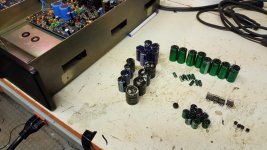
It looks like almost every capacitor on the Analog board is shorted or opened up. 13 of 16 caps have totally failed (dried up/overheated) or are so far out of tolerance (ie 135uF vs 470uF rated capacitance for example) are non-functional as designed.
I have a hard time believing that the seller tested this unit before he sold it to me. The thing smoked a few seconds after power was turned on.
What do you guys think? I am thinking he had the thing in storage for many years and just sold it to me without turning it on..
Any comments?
Thanks in advance
Could be. Hard to prove though. Also if that's what happened, hard to prove he would know, or should have known, it could be of any importance to say so.
Success! Final Update on Repair
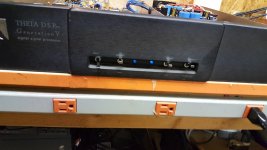
Success!
I have completed the repair successfully.
I recapped all of the electro caps as there were many failures on the Analog Board and some out of spec caps (smaller units) on Power Supply board.
It looks like the -30VDC & +30V (both regulated power supplies for the MPS8099/8599) had failed on one channel. One 1000uF 50V shorted and the other one opened up (lead separated from rest of body). This stressed one of the Negative regulator that measured really bad (120ohm from adjustable to output (after removed from PCB).
So I have a functioning Gen V Version A ( I thought I had bought a Gen V) but with the Green Wima caps/removed inductors at output & it looked like all the transistors were updated and matched. I assume I have the additional dither function that began with the Version A.
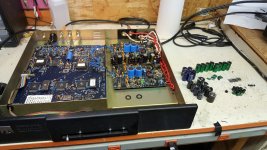
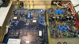
It has been running for an hour with no problems. Look at the attached photos that show the updated DAC and all the removed parts (mostly caps).
Success!
I have completed the repair successfully.
I recapped all of the electro caps as there were many failures on the Analog Board and some out of spec caps (smaller units) on Power Supply board.
It looks like the -30VDC & +30V (both regulated power supplies for the MPS8099/8599) had failed on one channel. One 1000uF 50V shorted and the other one opened up (lead separated from rest of body). This stressed one of the Negative regulator that measured really bad (120ohm from adjustable to output (after removed from PCB).
So I have a functioning Gen V Version A ( I thought I had bought a Gen V) but with the Green Wima caps/removed inductors at output & it looked like all the transistors were updated and matched. I assume I have the additional dither function that began with the Version A.
It has been running for an hour with no problems. Look at the attached photos that show the updated DAC and all the removed parts (mostly caps).
Attachments
Last edited:
Well done! These are excellent dacs but not easy to repair at all due to the lack of schematics etc.
Congrates! You may also check the bridge diode on 5V digital rail. I used to repair a burnt bridge diode on G3. It tends to be very hot during operation. BTW, the DAC can be improved vastly by newer regulators. However, this will definitely change the sound (same as recap anyway).
Congrates! You may also check the bridge diode on 5V digital rail. I used to repair a burnt bridge diode on G3. It tends to be very hot during operation. BTW, the DAC can be improved vastly by newer regulators. However, this will definitely change the sound (same as recap anyway).
I did replace the 2 Amp bridge with a 6Amp 800V Rectifier on the 5V Digital Rail as it looks like the 2A unit gets hot as per circuit board was slightly brown.
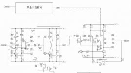
This is my physical drawing
Theta Gen V output stage circuit diagram, I don't know if it will help you.
Thanks for the schematic.... it will come in handy in order to understand the output stage...
Thanks,
Well done! These are excellent dacs but not easy to repair at all due to the lack of schematics etc.
A few more photos....
I will add power supply recap photo as I believe its on my home computer...
Attachments
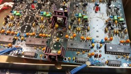

Are those tantalum caps all over that board? If so, that might be an area of upgrade as well.
What kind of caps would you use as an upgrade of these Tantalum caps ?
- Home
- Source & Line
- Digital Line Level
- Theta Gen V DAC Output Stage Issue: SCHEMATIC Anyone?