Boy I have really made this confusing. I have DN2535 MOSFETs. I thought you were referring to using two green LEDs in the test circuit for matching the JFETs. I see now that you were saying that the two green LEDs in the amp were providing a voltage reference.
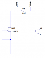
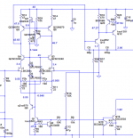
Back to a test circuit for matching the JFETs. Will the attached circuit work for testing and matching the 2SK170?
Thanks, Terry
Back to a test circuit for matching the JFETs. Will the attached circuit work for testing and matching the 2SK170?
Thanks, Terry
Attachments
Boy I have really made this confusing. I have DN2535 MOSFETs. I thought you were referring to using two green LEDs in the test circuit for matching the JFETs. I see now that you were saying that the two green LEDs in the amp were providing a voltage reference.
Back to a test circuit for matching the JFETs. Will the attached circuit work for testing and matching the 2SK170?
Thanks, Terry
Probably I wasn't clear enough when I said two LEDs voltage for matching. As keantoken said to use Vds of the same level the fets are under in the circuit, and that level is two LEDs voltage drop.
You can use your matching circuit, it is with 9 V instead 4 V, but it will make no difference. As 2sk170bl Idss is between 6 and 12 mA, on that resistor you will lose about 1 V.
BR Damir
I have a 2A DC supply that has 3V, 4.5V, 6V, 7.5, 9V, 10.5V & 12V settings. Would it be better to use the 4.5V setting? I have an ammeter setting on one of my DMMs if that would be more accurate.
I have a 2A DC supply that has 3V, 4.5V, 6V, 7.5, 9V, 10.5V & 12V settings. Would it be better to use the 4.5V setting? I have an ammeter setting on one of my DMMs if that would be more accurate.
You can use 4.5 V and than compare with 9 V, I think there would be no difference.
Hi Damir,
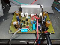
OK I have one board sort of working. It will play a sine wave but there is a lot of noise. It may be oscillating. If I hook my DMM to the ground and touch the other probe to the K-pin of Q14 the hiss sound will all but disappear. The only thing that is not installed are the two caps shown that go from the rails to ground right at the rail and ground studs. They are labeled C10 and C15 but on the schematic C15 & C15 are 470uf which I believe are C20 an C21 on the board. I will keep looking. It may be a have yet another solder bridge of cold joint somewhere. The bias is also very touchy. I have a ammeter hooked to the negative rail and the bias will jump from 30ma to 250ma in the blink of an eye so something is just not happy. More later after I've had a chance to do some more inspection.
Blessings, Terry
Attachments
Hi Damir,
OK I have one board sort of working. It will play a sine wave but there is a lot of noise. It may be oscillating. If I hook my DMM to the ground and touch the other probe to the K-pin of Q14 the hiss sound will all but disappear. The only thing that is not installed are the two caps shown that go from the rails to ground right at the rail and ground studs. They are labeled C10 and C15 but on the schematic C15 & C15 are 470uf which I believe are C20 an C21 on the board. I will keep looking. It may be a have yet another solder bridge of cold joint somewhere. The bias is also very touchy. I have a ammeter hooked to the negative rail and the bias will jump from 30ma to 250ma in the blink of an eye so something is just not happy. More later after I've had a chance to do some more inspection.
Blessings, Terry
Hi Terry,
Have you soldered 220pF ceramic C0G caps(C24, C19) directly between the pins base an collector of the drivers(Q95, Q95) on the PCB back side? Without them OPS will oscillate.
Also important is to connect input ground to the common star ground(outside the PCB).
Best wishes
Damir
No I didn't notice those. I will add them. Why attach the input ground to star? Doesn't that nulify the lifted ground?
I will do both, just want to understand.
Thanks, Terry
I will do both, just want to understand.
Thanks, Terry
No I didn't notice those. I will add them. Why attach the input ground to star? Doesn't that nulify the lifted ground?
I will do both, just want to understand.
Thanks, Terry
The lifted ground resistor just divide the power ground from the signal ground on the PCB, but both grounds should be connected to the common star ground.
As I said I am trying to learn. If you lift the input ground on the PCB but connect to the star anyway, what have you gained? Almost seems as though you may be creating a loop.
Another question, why, since you made a newer layout, didn't you fix all the component names so they matched the schematic and make a place for the two caps you are adding to the bottom of the PCB? This has been a rather difficult build.
Blessings, Terry
Another question, why, since you made a newer layout, didn't you fix all the component names so they matched the schematic and make a place for the two caps you are adding to the bottom of the PCB? This has been a rather difficult build.
Blessings, Terry
As I said I am trying to learn. If you lift the input ground on the PCB but connect to the star anyway, what have you gained? Almost seems as though you may be creating a loop.
Another question, why, since you made a newer layout, didn't you fix all the component names so they matched the schematic and make a place for the two caps you are adding to the bottom of the PCB? This has been a rather difficult build.
Blessings, Terry
Hi Terry,
I can try to explain how I see that thing about lifted ground. The main requirement is not to use the same ground for signal and power circuit on the PCB as power ground got dirty with power current pulses. I have seen first time that low value resistor between signal ground and power ground on JLH 80W mosfet amp. During PCB static testing you don't need to connect the signal ground to the common star ground, but when the amp is going to be test with a signal and a load then it is needed. If the signal ground is not connected to the common ground for a VFA amp it could be, probably, possible to play the music, but a CFA could have big problems as the feedback network is of much lower impedance. I fact you can just remove that lifting resistor connect all ground to the star ground. That resistor simplifies some testing. If someone does not agree with this please explain, I like to learn too.
Regarding the PCB errors. Terry you used the PCB I designed in 2012 and as nobody showed interest to build I did not check it carefully. You were to quick to develop the board and I did not have a chance to correct. For my amp I used two layers board I made before the one you choose, and that one was checked better but as double side not so simple for home make.
Regarding two bottom caps were described in the thread and you said you have read it thru.
By the way how is going with your test?
Best regards
Damir
I did read through the thread but I tend to miss some things because when things begin to get too technical for my understanding my eyes tend to glaze over.
I have not done any soldering yet today. Been at church all morning. I hope to get to it later today.
I have not done any soldering yet today. Been at church all morning. I hope to get to it later today.
As I said I am trying to learn. If you lift the input ground on the PCB but connect to the star anyway, what have you gained? Almost seems as though you may be creating a loop.
Another question, why, since you made a newer layout, didn't you fix all the component names so they matched the schematic and make a place for the two caps you are adding to the bottom of the PCB? This has been a rather difficult build.
Blessings, Terry
It's to isolate the (hopefully) quieter signal ground from the (probably noisier) power ground by eliminating a common return path. Doesn't take much to raise the noise floor of the amplifier by 10 db or more.
This jumps out at me watching the residuals of my distortion analyzer with an oscilloscope; it's not just a percentage, it's hum (60 Hz) and ripple (120 Hz and up), noise over the whole spectrum from audio to RFI, distortion products and sometimes, oscillation. Very often I use the low and high pass filters on my Tektronix AA501 analyzer to isolate hum and noise, and understand their contribution--a spectrum analyzer can bring out even more details. Incorrectly attaching test equipment can mess up measurements, and have you chasing false results--this happened to me last week.
A star-on-star ground within the power supply ground can reduce the charging pulses from the rectifiers/input capacitors by keeping the main star ground isolated. So it works both ways. In any case, attention to such details is becoming necessary because circuit design can lower distortion to the point that any source of hum and noise is now defining the ultimate performance of the amplifier. Layout of the pcb, general wiring and power supply needs careful attention, and it's hard for me to visualize, too.
This is becoming quite the challenge, to see how low we can go.
Hi Damir,
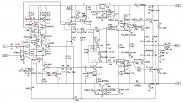
I'm having a problem with the front end. Q12 and Q20 have almost no VBE. The transistor check out OK. Any ideas are welcome.
Thanks, Terry
I'm having a problem with the front end. Q12 and Q20 have almost no VBE. The transistor check out OK. Any ideas are welcome.
Thanks, Terry
Attachments
Last edited:
Hi Damir,
I'm having a problem with the front end. Q12 and Q20 have almost no VBE. The transistor check out OK. Any ideas are welcome.
Thanks, Terry
Hi Terry,
Something is wrong with the LTP cascode biasing(Q3, Q4). On the D3 LED Anode should be close to 4 V(two LEDs voltage drop). Do the LEDs alight?
BR Damir
If you look at the base of Q3 and Q4 you will see 5.5V and emitter of Q9 is .544V so about a 5V drop. LEDs glow brightly.
VBE of of Q3 and Q4 is around .5V . VBE of Q5 & Q6 is about .6V.
However, vbe if Q15 is only .4v, vbe of Q20 is 0V and Q12 is .2V
I have checked and I have now shorts and the transistors are all good.
VBE of of Q3 and Q4 is around .5V . VBE of Q5 & Q6 is about .6V.
However, vbe if Q15 is only .4v, vbe of Q20 is 0V and Q12 is .2V
I have checked and I have now shorts and the transistors are all good.
Hi. dadod
i have a problem with schematic and component you can check something is wrong.
I'm not sure. The circuit working or error.
Thank you.
If you look at the base of Q3 and Q4 you will see 5.5V and emitter of Q9 is .544V so about a 5V drop. LEDs glow brightly.
VBE of of Q3 and Q4 is around .5V . VBE of Q5 & Q6 is about .6V.
However, vbe if Q15 is only .4v, vbe of Q20 is 0V and Q12 is .2V
I have checked and I have now shorts and the transistors are all good.
I simulated with your power supply voltage to see where are the voltage differences. What kind of a LEDs you use that you have 5V drop on them? Or maybe you have to high current, it should be about 3.1mA to 3.2mA through them.
On your attached schematic there is .147 on Q3 Q4 bases, but anyhow a transistor to conduct should have 0.6V or a bit more between base and emitter, 0.5V shows something is wrong.
I hope this ca help you, I still think that an error is in LTP and surrounding components or connections.
BR Damir
Attachments
Last edited:

Hi. dadod
i have a problem with schematic and component you can check something is wrong.
I'm not sure. The circuit working or error.
Thank you.
In principle it should work, but that is very old schematic and not very good one.
you are showing a reverse Vbe voltage across Q3&4Hi Damir,
I'm having a problem with the front end. Q12 and Q20 have almost no VBE. The transistor check out OK. Any ideas are welcome.
Thanks, Terry
- Status
- Not open for further replies.
- Home
- Amplifiers
- Solid State
- ThermalTrak+TMC amp