Thanks. The bump in low freq gain is not linked to R9-C5-C6. I can remove them completely and not cause the drop in loop gain (green -> blue). Cause is something more directly related to running the op amp from Vout...
BTW, shouldn't the "ESR boosting" resistor R9 really be between the caps and ground?
I will try changing to the universal op amp now.
BTW, shouldn't the "ESR boosting" resistor R9 really be between the caps and ground?
I will try changing to the universal op amp now.
Last edited:
Theoretically it may not matter -- if VOUT is indeed a perfect DC voltage that doesn't move even with fast risetime square wave output currents.
Practically, you want bypass capacitors across a fast opamp's supply pins. So put the isolation resistor to Vsupply and take advantage of the fact that 100 ohms x 10mA is only 1V of drop, which you can easily compensate for by increasing the level shifter voltage. 100 ohms in series with the opamp bypass cap(s), makes a series impedance which is so large relative to re' and Rload that it can be neglected at all frequencies. So you can focus your "output pole" analysis on the output capacitors and their ESR/ESL/explicit resistors.
Practically, you want bypass capacitors across a fast opamp's supply pins. So put the isolation resistor to Vsupply and take advantage of the fact that 100 ohms x 10mA is only 1V of drop, which you can easily compensate for by increasing the level shifter voltage. 100 ohms in series with the opamp bypass cap(s), makes a series impedance which is so large relative to re' and Rload that it can be neglected at all frequencies. So you can focus your "output pole" analysis on the output capacitors and their ESR/ESL/explicit resistors.
Thanks. I continued by replacing the op amp with universalopamp2 with
Avol=4K GBW=40Meg Slew=250Meg
ilimit=25m rail=0 Vos=0 phimargin=80
en=0 enk=0 in=0 ink=0 Rin=500Meg
(you were right re Avol - I just wasn't sure that Avol was where I put the open loop gain, presumably at DC)
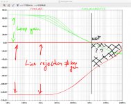
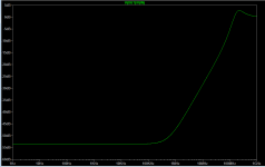
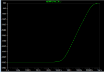
It did not change the behaviour noted above. There was a change to the phase plot versus the AD817A model but it was mostly out past 20MHz and the loop gain plot was very, very similar. Pic 1 shows the before and after of all the changes (combined). We see, principally, the unexplained behaviour re gain at low freq and the effect of the bypass cap pole at high freq.
Pic 2 plots line rejection and the bode plot for the 'idealised' circuit. The idealised circuit strips out the RCRC and so makes the point I raised above easier to see. I'm told 'loop gain is the gain available for error correction' and yet line rejection dB vastly exceeds loop gain dB at any given frequency. More so, line rejection continues beyond the UGF where loop gain is 1. I'm sure the explanation is basic but I am missing it.
Secondly, playing with the 'output capacitance pole' simply by stepping Cout doesn't change line rejection - or at least not significantly - for those frequencies with increased loop gain. Presumably the extra loop gain there isn't enough to move the total line rejection needle. Counterintuitively for me, given the foregoing, we can see the impact from what I presume to be the changing output cap ESR pole which alters the loop gain plot well above the UGF and a corresponding readily visible change in the line rejection plot.
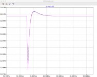
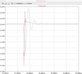
I also don't understand why dropping the two output caps from 470u each to 47u each offers no appreciable change in the transient waveform (see attached 0.1A->0.6A load transient). I distinctly remember going for the dual and higher output capacitance in the MOSFET design because I thought it helped transient response and output impedance but a revisit of those models suggests no gains from doing so. It's as if the Cout discharge is instantaneous and identical in all cases. Perhaps I am just going mad... again. What the analysis does suggest is that I find the smallest output cap, with the finest pin pitch to minimise inductance, that still maintains stability.
Avol=4K GBW=40Meg Slew=250Meg
ilimit=25m rail=0 Vos=0 phimargin=80
en=0 enk=0 in=0 ink=0 Rin=500Meg
(you were right re Avol - I just wasn't sure that Avol was where I put the open loop gain, presumably at DC)
It did not change the behaviour noted above. There was a change to the phase plot versus the AD817A model but it was mostly out past 20MHz and the loop gain plot was very, very similar. Pic 1 shows the before and after of all the changes (combined). We see, principally, the unexplained behaviour re gain at low freq and the effect of the bypass cap pole at high freq.
Pic 2 plots line rejection and the bode plot for the 'idealised' circuit. The idealised circuit strips out the RCRC and so makes the point I raised above easier to see. I'm told 'loop gain is the gain available for error correction' and yet line rejection dB vastly exceeds loop gain dB at any given frequency. More so, line rejection continues beyond the UGF where loop gain is 1. I'm sure the explanation is basic but I am missing it.
Secondly, playing with the 'output capacitance pole' simply by stepping Cout doesn't change line rejection - or at least not significantly - for those frequencies with increased loop gain. Presumably the extra loop gain there isn't enough to move the total line rejection needle. Counterintuitively for me, given the foregoing, we can see the impact from what I presume to be the changing output cap ESR pole which alters the loop gain plot well above the UGF and a corresponding readily visible change in the line rejection plot.
I also don't understand why dropping the two output caps from 470u each to 47u each offers no appreciable change in the transient waveform (see attached 0.1A->0.6A load transient). I distinctly remember going for the dual and higher output capacitance in the MOSFET design because I thought it helped transient response and output impedance but a revisit of those models suggests no gains from doing so. It's as if the Cout discharge is instantaneous and identical in all cases. Perhaps I am just going mad... again. What the analysis does suggest is that I find the smallest output cap, with the finest pin pitch to minimise inductance, that still maintains stability.
Attachments

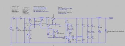
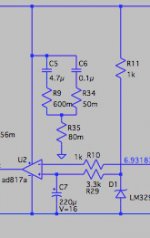
Note in the model R9 is 0.1R rather than 100R - just enough to remove the instability caused by the bypass caps. The 4.7u tantalum cap I use has max ESR @ 100kHz of 600m Ohms. I'm not sure about the 100n COG ceramic but I understand the series resistance of ceramics is extremely small in general. In the Sziklai build the equivalent of R9 was just a zero ohm jumper. I think I will just change the model to have an explicit series resistance of 0.6R in series with the 4.7u cap.
Good. The Green/Red plot provides an excellent practice area in which to hone your diagnostic skills and detective instincts.
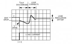
Understanding why the output capacitors don't produce the expected effect during transients, might be made easier if you explicitly drew the RLC model of each electrolytic capacitor right on the LTSPICE schematic. That way you can probe internal nodes "inside" the capacitor, and in particular, you can plot the deltaV across ESR, plot the deltaV across ESL, and so forth. Another handy fact is Kirchoff's Current Law which states that sum(currents in) equals sum(currents out) of each node. At the output node, Iload = Iemitter + Icap + errors. Plotting these currents may yield Eureka. Decreasing C by 4X has no effect upon Icap? It gives one furiously to think, Captain Hastings.
Understanding why the output capacitors don't produce the expected effect during transients, might be made easier if you explicitly drew the RLC model of each electrolytic capacitor right on the LTSPICE schematic. That way you can probe internal nodes "inside" the capacitor, and in particular, you can plot the deltaV across ESR, plot the deltaV across ESL, and so forth. Another handy fact is Kirchoff's Current Law which states that sum(currents in) equals sum(currents out) of each node. At the output node, Iload = Iemitter + Icap + errors. Plotting these currents may yield Eureka. Decreasing C by 4X has no effect upon Icap? It gives one furiously to think, Captain Hastings.
Good. The Green/Red plot provides an excellent practice area in which to hone your diagnostic skills and detective instincts.
I knew you were going to say something like that 🙂
These two articles offer clues:
http://www.ti.com/lit/an/slyt202/slyt202.pdf
Understand Low-Dropout Regulator (LDO) Concepts to Achieve Optimal Designs
First, it seems it is not Loop Gain that matters but Open Loop Gain. Here the difference between AOL and Loop Gain i.e. 1/B, is only a few dB (4.8dB is what I calculated) but it helps explain the extension of PSRR beyond the UGF. It also seems that there is a multiplier effect as a result of the less than unity gain from Vin to Vout.
PSRR = 20Log(Aol/Avo)
where Aol = open loop gain and Avo = the gain from Vin to Vout with the loop open
I'm still trying to get my head around these points...
The little degradation of PSRR at very low frequencies is due to an imperfect Vref - I get that.
I've also learnt that beyond the UGF the output caps dominate alongside parasitics from Vin to Vout. This explains why we see variations in PSRR in very high frequencies as we vary Cout. Ok fine.
I presume that the reason why changing Cout doesn't affect PSRR at sub UGF frequencies where it does affect loop gain is because the open loop gain of the op amp isn't changed. The corollary being the poles and zeros we've been discussing are relevant only to the closed loop response, loop gain (which makes sense).
I think I will leave it at that for today...
I will work through the output cap/transient issue and try to tackle your homework assignment in the next couple of days. In the interim, I read this again and I think you are saying just go ahead and use 100R in the circuit and "kick the issue into touch" i.e. use 100R, there's little cost in terms of voltage to the op amp and you don't need to worry about the Cbypass pole. I guess the lower supply range will mean a bit lower open loop gain.
Practically, you want bypass capacitors across a fast opamp's supply pins. So put the isolation resistor to Vsupply and take advantage of the fact that 100 ohms x 10mA is only 1V of drop, which you can easily compensate for by increasing the level shifter voltage. 100 ohms in series with the opamp bypass cap(s), makes a series impedance which is so large relative to re' and Rload that it can be neglected at all frequencies. So you can focus your "output pole" analysis on the output capacitors and their ESR/ESL/explicit resistors.
Last edited:
I haven't forgotten about this. Due to family commitments I've had little time the last two weeks. The little I have had has been tempted by beginning assembly of my SA2014 amp designed by duyAudio member astx. Hopefully I can resume next week.
Here I step Cout from 470u->220u->100u->47u. The pole shifts higher in frequency creating more loop gain between 100Hz and 100kHz. .... There's also no change to output impedance or transient response with varying Cout which isn't my recollection from modelling the MOSFET pass transistor configuration. 😕
Understanding why the output capacitors don't produce the expected effect during transients, might be made easier if you explicitly drew the RLC model of each electrolytic capacitor right on the LTSPICE schematic. That way you can probe internal nodes "inside" the capacitor, and in particular, you can plot the deltaV across ESR, plot the deltaV across ESL, and so forth. Another handy fact is Kirchoff's Current Law which states that sum(currents in) equals sum(currents out) of each node. At the output node, Iload = Iemitter + Icap + errors. Plotting these currents may yield Eureka. Decreasing C by 4X has no effect upon Icap? It gives one furiously to think, Captain Hastings.
Yes I see the differences in Icap with varying Cout and trivial change to the Vout transient. Of course, varying Cout (leaving number of caps, Lser and Rser constant) is not the same as dropping one of the caps out of the circuit - this does have a massive effect on transient response. I will leave the output caps as they are.
Practically, you want bypass capacitors across a fast opamp's supply pins. So put the isolation resistor to Vsupply and take advantage of the fact that 100 ohms x 10mA is only 1V of drop, which you can easily compensate for by increasing the level shifter voltage. 100 ohms in series with the opamp bypass cap(s), makes a series impedance which is so large relative to re' and Rload that it can be neglected at all frequencies. So you can focus your "output pole" analysis on the output capacitors and their ESR/ESL/explicit resistors.
I wonder if this is so easy. Here I have reconfigured the op amp bypass caps C5 and C6 to explicitly add an assumption as to their ESR. Using a 100R "isolation resistor" (R47) produces the unusual red trace. Leaving it out (approximated by assuming 1p) produces the turquoise trace which is clearly underdamped. But perhaps my assumptions for the two caps' respective ESR is invalid. The 4.7u tantalum caps from AVX have a typical impedance at 100kHz of 700mR. (I used 600m to provide some conservatism.) I have no idea what is a valid assumption for the COG or X7R 0.1uF ceramic but I understand their ESR to be inherently very small - I used 50mR here. The level of damping seems better finessed by a trailing series resistor (R35). In the physical Sziklai circuit which was tested "R47" was jumpered with a zero Ohm resistor and there was no trailing series resistor.
Attachments
It might be time to disconnect the opamp's power supply input terminal from this RC network and supply the opamp from an ideal voltage source. This could let you know whether misbehavior is caused by the passive components alone, or caused by the interaction between the opamp and the passive components.
I assume you have asked yourself: if the circuit really does include a preregulator, what about powering the opamp from the relatively clean pregegulated supply?
I assume you have asked yourself: if the circuit really does include a preregulator, what about powering the opamp from the relatively clean pregegulated supply?
Yes I have, but it seems like this might well be solvable when powered from Vout, even if only by empirical observation. The isolation resistor provides a handy place for connecting a wire jumper from Pre-reg_out should it not work. And maybe someone will want to try this circuit without the pre-reg.
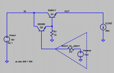
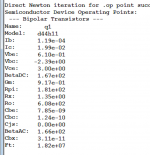
I am stuck on your homework assignment. I calculated the (open) loop gain of the circuit as 77.8dB at low frequencies. (I broke the loop just after Rout_OL_AD817, injected an small AC signal of 1 and computed Vout/V(Y) where Y is "to the right" of the injection stimulus.) I calculated an input ripple rejection of 60.4dB at similar frequencies. (This differs from what you got - perhaps we have different models for the D44H11?) The ratio of the latter to the former is 13%.
I understand how the simple regulator circuit works in principle but I am struggling to explain the relationship between loop gain and input ripple rejection or the significance of Rout_OL_AD817.
Also I am struggling to see the relationship between the calculated loop gain and hfe. I would have thought them closely related. Yet even when I strip out the driver transistor the increased loop gain calculated bares little resemblance to the hfe charts for the D44H11. 😱
D44H11 model I am using:
**************************************
* Model Generated by MODPEX *
*Copyright(c) Symmetry Design Systems*
* All Rights Reserved *
* UNPUBLISHED LICENSED SOFTWARE *
* Contains Proprietary Information *
* Which is The Property of *
* SYMMETRY OR ITS LICENSORS *
* Modeling services provided by *
* Interface Technologies Interface Technologies – Engineering Software and Services *
**************************************
.MODEL Qd44h11 npn
+IS=6.99994e-12 BF=91.0001 NF=1.04634 VAF=40.7259
+IKF=10 ISE=7e-11 NE=3 BR=1.97064
+NR=1.50008 VAR=22.902 IKR=35.9467 ISC=4.75e-12
+NC=3.59375 RB=4 IRB=0.1 RBM=0.1
+RE=0.0001 RC=0.130733 XTB=0.337319 XTI=1.40625
+EG=1.13125 CJE=1.03578e-09 VJE=0.651779 MJE=0.35303
+TF=3.07008e-09 XTF=1.35721 VTF=0.995654 ITF=1
+CJC=3.98764e-10 VJC=0.429208 MJC=0.35114 XCJC=0.803125
+FC=0.533449 CJS=0 VJS=0.75 MJS=0.5
+TR=4.30593e-07 PTF=0 KF=0 AF=1
* Model generated on Mar 1, 2004
* Model format: PSpice
It might be time to disconnect the opamp's power supply input terminal from this RC network and supply the opamp from an ideal voltage source. This could let you know whether misbehavior is caused by the passive components alone, or caused by the interaction between the opamp and the passive components.
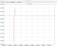
Hmm. Disconnect the bypass caps and one gets the behaviour in the red trace (above in post 291). Supply the op amp from an ideal 12V source - with or without the bypass caps - and one gets the same. Alternatively, a direct connection to Vout, with the bypass caps and with a trailing series resistor of 80m produces the result below.
Attachments
There is no loop to break in post #287. Because there is no loop, the "loop gain" is zero. (minus infinity dB).
There is no feedback and there is no "regulation" .
Even so, there IS attenuation from rawDC input to "regulated" output. This is the Eureka! observation which answers the question in post #283: Why is line rejection not equal to loop gain?
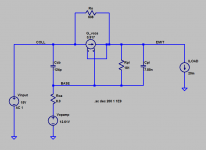
edit- as its name implies, an emitter follower circuit causes its emitter voltage to follow its base voltage. An emitter follower circuit theoretically ignores any signals present on its collector voltage. you are putting an input signal on the D44H11 collector and measuring the output at the emitter. in theory we expect zero output. cordell figure 2.3 is worth studying again.
There is no feedback and there is no "regulation" .
Even so, there IS attenuation from rawDC input to "regulated" output. This is the Eureka! observation which answers the question in post #283: Why is line rejection not equal to loop gain?
edit- as its name implies, an emitter follower circuit causes its emitter voltage to follow its base voltage. An emitter follower circuit theoretically ignores any signals present on its collector voltage. you are putting an input signal on the D44H11 collector and measuring the output at the emitter. in theory we expect zero output. cordell figure 2.3 is worth studying again.
Last edited:
I agree there is no loop. I should not have said "broke the loop". Rather I should have said "broke the circuit".
("There is no feedback" - I guess this is the debate about whether a zener is a "regulator". But it is beside the point here.)
Ok so line rejection is equal to the sum of closed loop gain of the feedback circuit plus the "attenuation" component. The latter is a function of frequency also. Is this not determined by the gain profile of the Darlington configuration? This is what I was attempting to model when I broke the circuit at RL_Out_AD817 and injected a small signal AC of 1. I was expecting a ratio of 1.
An op amp's open loop gain profile is with the feedback loop open. (Feedback reduces this to closed loop gain or more simply "loop gain".) I've been trying to think about the attenuation component in like terms and failing miserably.
Sounds like you now understand the green line and red line in plot 2 of post #283, congratulations.
An emitter follower circuit's ability to prevent collector waveforms from appearing on the emitter, does not extend to infinite frequencies of course. You could try simulating a single transistor or a two transistor circuit like post #287 to see whether changing the transistor fT changes the shape of input ripple rejection vs frequency. Or you could simply declare "question answered" and move on.
If you suspect that LTSPICE is doing nonsensical things, you could try (i) switching to the Alternate solver; (ii) switching to the Gear integration method; (iii) setting .OPTIONS MAXSTEP to something small like perhaps 1/3rd of (1/opampGBW), i.e., 6.7 nanoseconds; or combinations of these. Probably you'll get the exact same answer no matter what changes you try, but actually seeing it happen will be reassuring.
Thanks to your help.
For now, I'd be happy to understand how to estimate the attenuation at low frequencies (even for a single transistor EF setup). I only understand the mechanism of the attenuation in the broadest possible terms: the pass transistor 'locks' (as best it can) Vout at 2 Vbe (for this circuit) below the "reference" voltage provided by Vop amp (less the drop over ROUT_OL_AD817). The pass transistor acts as a "variable resistor". The texts I have seem to gloss over the detail as they move quickly to more complex regulator circuits. They provide examples where a Zener diode sets Vref, note that Vbe still fluctuates with Vin and move on. There's no explanation as to the magnitude of regulation/attenuation by freq. (BTW I stepped fT but the result was the same.)
I had been using the alternate solver; the result is the same with the normal solver. I tried also (iii) above. No change. I've added space on the board for both the 'isolation resistor' and a trailing ESR boosting resistor. I think I will just order them and make up the Darlington version for testing.
EDIT: I found this informative discussion: http://etc.unitbv.ro/~craciun/DCE/Course/VoltReg.pdf
I seem to be able to replicate somewhat the low freq attenuation estimate in an example whereby I replace Q2 with a 1K resistor and drive the base of Q1 from ROUT_OL_AD817 (also deleting R1). LTspice suggests -41.17dB of attenuation which is 'close' to 8/1k. I assume parasitics in the pass transistor interact to affect the result and cause the rolloff in attenuation at higher frequencies.
The homework example is obviously more complex but it is no longer surprising that simply varying the fT of the pass transistor doesn't alter the degree of attenuation.
Cordell Figure 2.3 shows that there are two pathways for (signals on the collector) to find their way to the emitter. One of them is an infinitely high impedance and the other is not. Analyzing these situations is what circuit designers do for a living.
_
_
Attachments

Luckily, I don't need to make a living from this else I'd starve. I understand that this is a small signal model and variables will change for each operating point. But I was still expecting Vemit to be one Vbe below Vbase. It isn't. And I still can't compute the -54.6dB of attenuation at low frequencies nor the 3dB point of c272kHz. I'll keep at it.
- Status
- Not open for further replies.
- Home
- Amplifiers
- Power Supplies
- Thermal considerations for Fairchild SDIP bridge rectifiers