Since the NPN base current is very small, it doesn't make a lot of difference whether your current source is set to 6mA or 10mA or 15mA, as long as you don't squirt in more than the opamp's output stage can drink. And the AD817 is beefy and robust in this regard.
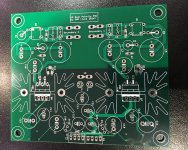
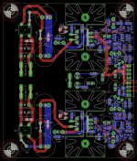
All SMD soldering done and just the +ve half of the reg through-hole soldering done. I will test this first without the rectifier components populated and with my bench PSU connected ahead of the first filter resistor. We'll see if there's smoke!
Hmm. After an initial hiccup it seems to work! I'm a little surprised as my "hiccup" was a 4.7uF tantalum cap soldered around the wrong way. (Perversely, I was very conscious of polarity but stupidly 'misread' my PCB layout. Memo to self, for tantalum caps place a polarity marker on the PCB silk!) I'm surprised other components survived the destruction of the cap and rapid rise in current to a couple of amps or so (according to the display on my bench PSU) given the problem was downstream of most components as the supply for the op amp is from the output of the pass transistor. The trimmer resistor works to adjust Vout of the LM2941 pre-regulator.
I now need to couple up a scope and do some transient testing with a certain chop chop box...
I now need to couple up a scope and do some transient testing with a certain chop chop box...
Last edited:
Get a Variac. It will let you slooooooowly turn up the mains voltage while watching the AC ammeter. Too much current? Stop, turn it back to zero, and go searching.
Amazon example priced at £38.95
Amazon example priced at £38.95
Good idea. Although in this case I should have simply set the current limit on my bench PSU which I was using to inject 18Vdc just downstream of the as yet unpopulated rectifier. Lesson learnt hopefully. The bit I am puzzled about is that I am sure that by the time I flicked the switch on my bench PSU the current was above 2A - above the short circuit current of the LM2941. No obvious signs of damage to any other component though and the trimmer still alters Vout of the first stage.
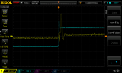
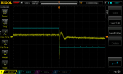
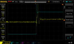
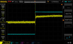
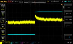
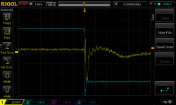
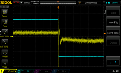
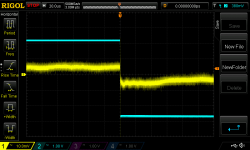
I did some transient tests using Mark's chop chop box.
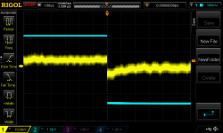
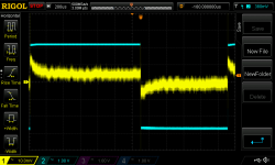
For the images below the blue trace is probing the trigger on the chop chop box while the yellow trace is probing the output of the regulator using probe point and ground 'spring' (except for image 5):
1. Load off waveform. Seems like not a bad reaction to a 0.48A transient load.
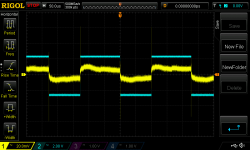
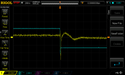
2-4. Load on waveform, zooming in.
5. Probing the base of the D45VH11 pass transistor. I have no base stopper resistors installed i.e. R25 is a zero Ohm jumper. (See circuit in post 175)
6. I have added a closer look at the overall waveform as pic 2 looks rather disturbing?
For the images below the blue trace is probing the trigger on the chop chop box while the yellow trace is probing the output of the regulator using probe point and ground 'spring' (except for image 5):
1. Load off waveform. Seems like not a bad reaction to a 0.48A transient load.
2-4. Load on waveform, zooming in.
5. Probing the base of the D45VH11 pass transistor. I have no base stopper resistors installed i.e. R25 is a zero Ohm jumper. (See circuit in post 175)
6. I have added a closer look at the overall waveform as pic 2 looks rather disturbing?
Attachments

Last edited:
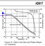
Looks like ESR+ESL isolates the output capacitor from the load for the first ~20 nanoseconds, causing overshoot spike. The damping appears to be a bit less than critically damped; as a wild-azssed guess I'd say zeta=0.5.
From the graphs in this old post, zeta=0.5 corresponds to about 50 degrees of phase margin, or thereabouts.
So, it's stable. You're done.
If you want to reduce the height of the overshoot spike, I suspect you'll need to reduce ESR+ESL which will affect stability since it changes the output zero. You may need to reduce the unity gain crossover frequency to keep the whole thing stable.
Hi. I'm already using two low ESR caps at the output (the EEU-FR1E471L are rated 0.030 Ohms impedance at 100kHz) and I understand the impact of changing the output caps on the output zero. So I suspect there isn't much to play with there although I am most probably mistaken 🙂
Rightly or wrongly the pics I was most concerned with were those of the overall waveform, pics 2 and 6 as it seems the regulated output never really "flat lines"...
At this stage there is no compensation capacitor fitted now any base stopper resistor.
Rightly or wrongly the pics I was most concerned with were those of the overall waveform, pics 2 and 6 as it seems the regulated output never really "flat lines"...
At this stage there is no compensation capacitor fitted now any base stopper resistor.
This might be addressed by (a) slowing down the input square wave frequency by a factor of 10X; and (b) using 16X averaging from the scope Acquire menu. If the Vout trace never flatlines even after a very VERY long time then you do indeed have trouble. You could also add a fixed resistor between Vout and GND, which increases the quiescent bias current. I'd consider making it (Vout / 0.01) ohms; viz., for 12V output I'd consider 1200 ohms.... the pics I was most concerned with were those of the overall waveform, pics 2 and 6 as it seems the regulated output never really "flat lines"...
This might be addressed by (a) slowing down the input square wave frequency by a factor of 10X; and (b) using 16X averaging from the scope Acquire menu. If the Vout trace never flatlines even after a very VERY long time then you do indeed have trouble. You could also add a fixed resistor between Vout and GND, which increases the quiescent bias current. I'd consider making it (Vout / 0.01) ohms; viz., for 12V output I'd consider 1200 ohms.
I never did figure out how to calculate the frequency of your Schmitt trigger oscillator circuit given the hysteresis deployed. Nonetheless, I assume that changing R11 to 10K ought to slow down the frequency of oscillation sufficiently for this exercise. (circuit here)
Regarding the quiescent bias current, I have bleeder resistors to LED to GND at the output caps. However, I just upped the values of these from 1k to 2.49k as the LED were unnecessarily bright and I was wanting to conserve current. My bench PSU displays 0.05A with no load attached.
Much easier and safer to increase timing capacitor C7 by 10X; just tack solder the new parallel capacitor across the leads on the bottom side of the board. After all this is a quick and dirty experiment, whose only purpose is peace of mind.
On the other hand the timing resistor is engaged in a tug-of-war against the positive feedback network. If you increase the timing resistor while leaving the other two resistors alone you might prevent it from winning the war and thus, never oscillating.
On the other hand the timing resistor is engaged in a tug-of-war against the positive feedback network. If you increase the timing resistor while leaving the other two resistors alone you might prevent it from winning the war and thus, never oscillating.
Ok. Even easier as C7 is socketed.
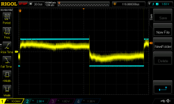
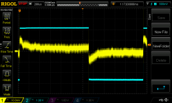
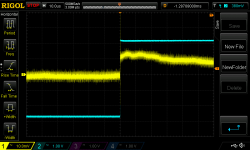
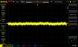
Seems very noisy...
Seems very noisy...
Attachments
Last edited:
The yellow fuzz looks about the same in both load conditions, so you don't need the chop box to make fuzz appear. If that fuzz really is oscillation you can turn off the chop box and go track it down with a constant load.
Your regulator ought to have a very low output impedance at 430 Hz (11.5 divisions X 200us/division) so I'm surprised that dI=0.5 amps causes dV=0.003 volts. That means Zout is 6 milliohms which seems terribly low. Is there a chance you're measuring the yellow waveform with the ground connection not quite at the correct spot? The correct spot is the place where R39 connects to the anode of Z3 (in post #175).
Your regulator ought to have a very low output impedance at 430 Hz (11.5 divisions X 200us/division) so I'm surprised that dI=0.5 amps causes dV=0.003 volts. That means Zout is 6 milliohms which seems terribly low. Is there a chance you're measuring the yellow waveform with the ground connection not quite at the correct spot? The correct spot is the place where R39 connects to the anode of Z3 (in post #175).
Here are a series of scope shots probing the V+ of X6 with the ground spring in R39's via to ground.
Attachments
-
 NewFile45.png34.9 KB · Views: 68
 -
 NewFile44.png44 KB · Views: 66
 -
 NewFile43.png43.5 KB · Views: 74
 -
 NewFile42.png44.4 KB · Views: 75
 -
 NewFile39.png34.9 KB · Views: 70
 -
 NewFile38.png43.5 KB · Views: 68
 -
 NewFile37.png43.1 KB · Views: 91
 -
 NewFile36.png43.7 KB · Views: 103
 -
 NewFile35.png45.7 KB · Views: 94
One other thing, it seems like this regulator is much 'slower' to react to a load change - even putting the lower damping factor to one side for a moment - than my previous MOSFET-based reg... (link to similar tests for that reg) Both use the same output caps. I would have expected the BJT series pass transistor to give significantly faster response given its faster gm...
1. Oops, typing while thinking leads to errors. Zout=6 milliohms seems terrible, i.e., terribly HIGH. I expect something more like (1 ohm) / (open loop gain at 430 Hz) = 1/(70dB) = (1/3160) = 0.3 milliohms.
2. Glad to hear that the fuzz is a measurement artifact and not a property of the voltage regulator
3. Simulation may be able to tell you how "slow to react" the two designs "should" be. Remember that the BJT Sziklai output stage uses a common emitter PNP amplifier stage (Q7 in post #175) to deliver the majority of the output current, which might or might not be slower than a common source NMOS follower stage.
4. Selecting Averaging=16X on the oscilloscope's Acquire menu, might reduce the height of the fuzz.
_
Attachments
Hmm ok. I'm also grappling with the other side of the regulator which I wanted to get working as a means of comparison. But it's not working. I'm dropping 4V across R36 and so Vref at D4 via is 3V instead of 7.1V at the LM329. I have replaced R36, the pass through cap and the op amp trying to find the issue but no luck so far. I'll replace D3 and D4 next.
- Status
- Not open for further replies.
- Home
- Amplifiers
- Power Supplies
- Thermal considerations for Fairchild SDIP bridge rectifiers