ClassII rules
a.) The enclosure (or biggest metal part) must be permanently connected to PE.
b.) All exposed conductive parts should be connected to the protected enclosure.
Note that neither a.), nor b.), require one to use a metal enclosure.
Note also that exposed metal part/s, eg. RCA/Phono barrels and screw heads/nuts on the ouside should be connected to Safety Earth (the protected chassis/enclosure)
better, but isolated fixing holes through the PCB would also achieve the same......What's the best way to have the circuit float? Just use nylon standoffs instead?
If heat dissipation from the underside is not an issue then you could glue the PCB to the side wall or to the floor with a thick layer of silicone window sealant.
That's the way I "fix" my big smoothing capacitors.
Note also that exposed metal part/s, eg. RCA/Phono barrels and screw heads/nuts on the ouside should be connected to Safety Earth (the protected chassis/enclosure)
With a metal chassis, doesn't this connect signal ground to safety earth? Do you mean for jacks with a metal D-shape housing?
better, but isolated fixing holes through the PCB would also achieve the same.
What's an isolated fixing hole and how do I make one? 😱
If heat dissipation from the underside is not an issue then you could glue the PCB to the side wall or to the floor with a thick layer of silicone window sealant.
That's the way I "fix" my big smoothing capacitors.
How's this work out for you when you need to replace or swap the PCBs after?
design build and test your audio outside your chassis. Get it all working and record all your test results. Then fold it all up into it's final "shape" and install it in the enclosure. At this stage the audio should still be "floating".With a metal chassis, doesn't this connect signal ground to safety earth? Do you mean for jacks with a metal D-shape housing?
Add in the Safety connection that meets rule b.)
Re-test to see what performance results have been matched and what has deteriorated. I have NEVER got improved performance by fitting inside a metal chassis !
a hole that has no component and no trace nearby. I don't know why some layout designers add a copper pad around a PCB fixing hole !What's an isolated fixing hole and how do I make one? 😱
You can peel the silicone off (with difficulty). Maybe just doing the corners might be more reversible.How's this work out for you when you need to replace or swap the PCBs after?
Alternatively, for any mains PCB (DC blocker and soft start).
I attach a thick plastic sheet to the trace/solder side of every mains PCB. This is to prevent accidents, tools/fingers/chassis.
That plastic sheet could then be glued to the chassis.
Owen,
First, I love your work. I built the SE-SE l loved it so much I built BAL-BAL and now I'm in process of building the LPUHP.
I have yet another BAL-BAL volume pot question.
I have both SE-SE and BAL-BAL wired the same way, though the latter uses a stepped attenuator.
My source is Sonic Frontiers SFD-1 Mk II. The SE output works great, but I'm really having issues with the balanced out.
The pot is 10K and initially I kept the Rf/Ri as per specification. Unfortunately the volume was at around 75% of the desired one and after reading all mentions of potentiometer and pot in the thread I decided to a) increase gain and b) increase the Rf/Ri values.
I went for Rf=20K and Ri=10K.
Now the maximum output value is at 40%.
What did I do wrong?
Was it just my inexperience or there are specifics with the tube output stages?
Why does the SE-SE work normally?
BTW, SFD-1 is not "real" balanced DAC as it only has 1 chip and 2 tubes (vs SFD-2, which is truly balanced).
I would really appreciate help with this.
Lucho
I have yet another question... my amp was working wonderfully for a while, minus an occasional potentiometer short. I finally got around to reflowing that joint today, and that's all I did, but now I'm getting noticeable hum when I turn the volume up, and a small pop/buzz if I touch the knob. I'm assuming this is a grounding issue as well, but I'm not sure where to start looking 😱
^ Nevermind, I actually think the power I was getting from the wall was particularly noisy for a variety of reasons. Listening at a quieter time of day I get almost no hum until max volume on very sensitive earbuds.
OPC, the BAL-BAL boards arrived. Thanks. Can I check the wiring? "Out" seems straightforward but there are no polarity markings on the supply input. I'd rather ask than make a mistake. If the board is oriented with the OPAs at the front and the silk text is 'right way up', which hole is V+ and which is V-? Pics of builds here suggest V- is on the left and V+ on the right but then those boards have markings on the silk to that effect as well whereas mine don't. On the signal input, what's the middle hole for?
EDIT: post 2257 has a pic of what appears to be Pin 1 being connected to signal ground if that's what the middle of the three holes at the input to the amp module is. That would be a huge mistake, no? XLR pin 1 should only be connected to the chassis. Pin 1 is for shielding, it is not for signal.
EDIT: post 2257 has a pic of what appears to be Pin 1 being connected to signal ground if that's what the middle of the three holes at the input to the amp module is. That would be a huge mistake, no? XLR pin 1 should only be connected to the chassis. Pin 1 is for shielding, it is not for signal.
Last edited:
SGK,
you are right.
We have been told for over 20years how to wire Pin1 and yet we still find folk wiring it wrongly.
Pin1 goes to chassis.
you are right.
We have been told for over 20years how to wire Pin1 and yet we still find folk wiring it wrongly.
Pin1 goes to chassis.
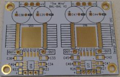
Hi SGK,
I just had a close look at the boards and realized the PCB fab house made a total mess of the silkscreen on the power inputs. They are on the board, but in the wrong spot, making them impossible to read.
I have attached a picture of the board with the correct silkscreen which should help you identify the power inputs. I will also add this to the Wiki for clarity.
The signal inputs are as marked, and the middle pin connects to audio ground.
This was done for flexibility, so please feel free to hook these up in whatever way you see fit. You don't need to terminate a GND here, but please be mindful of the common mode DC limitations if you do long runs without any GND reference.
Regards,
Owen
Attachments
Thanks Owen. I just looked at the spare board I purchased and indeed I can see the markings buried in the silk for the caps - I had already soldered the caps (and everything else) and so they were covered up. Is the Wiki working now? I haven't been able to get it to work for some time now.
I don't follow this. Can you explain? We have a differential signal input and differential output. + is referenced to - and not to any "GND".
(BTW soldering the heat sinks was a b*$%@! Any tips if I ever have to do it again? I did these last but feel like I should have done them before the caps and used solder paste and a heat gun.)
but please be mindful of the common mode DC limitations if you do long runs without any GND reference.
I don't follow this. Can you explain? We have a differential signal input and differential output. + is referenced to - and not to any "GND".
(BTW soldering the heat sinks was a b*$%@! Any tips if I ever have to do it again? I did these last but feel like I should have done them before the caps and used solder paste and a heat gun.)
I don't follow this. Can you explain? We have a differential signal input and differential output. + is referenced to - and not to any "GND".
Internally, the op-amp is referenced to GND, and the common mode DC offset at the input is limited to roughly the supply voltage. If the voltage at either input pin exceeds the supply voltage relative to GND, then the op-amp can be damaged.
Imagine you run only the two differential wires from your preamp to the input of the headphone amp which sits all the way across the room on another outlet/circuit, thereby omitting any GND reference between the two units. If the GND reference for the amplifier ever differs from the GND reference of the source, then this will appear on the input of the headphone amp as a common mode offset. If this is only a few volts (eg, both chassis are earthed and connected to the same power bar) then this won't be a problem. If both units are not earthed, or far away from one another, then getting more than 15V differential between the two GND references could easily happen due to line transients, ESD, or inrush current. Under these circumstances, the op-amp is at risk. Always make sure there is some solid common GND reference between the source and the amp. Generally, this is done with pin 1 which would link both chassis together at the output and input.
(BTW soldering the heat sinks was a b*$%@! Any tips if I ever have to do it again? I did these last but feel like I should have done them before the caps and used solder paste and a heat gun.)
These are indeed a pain... the best way is to use paste and bake the whole thing, but I just used an 80W iron with a 3mm flat tip and it went pretty well. Once one side is tacked down I was able to solder the other fully without the heatsink moving around.
Regards,
Owen
excessive common mode voltage
SGK,
there are three alternatives that I can see.
a.) Install the interconnect with screen/shield connected to Pin1 at both ends and Pin1 connected to Chassis at both ends.
b.) design the circuit inputs to tolerate excessive common mode voltage on the signal lines. This is usually discussed in the datasheet. Many inputs have protection built into the IC chip and the datasheet gives guidance on what impedance/resistance to put into the signal lines to prevent the internal protection from becoming damaged.
c.) do neither of the above and hope the circuit survives.
Yes (a) is the right solution. I just don't think of this as a "GND reference". It merely ensures that both chassis are at more or less the same potential. The only signal reference is the other half of the +/- transported via pins 2 and 3. Better XLR connectors ensure the cable shield and the whole connector shell meet with the chassis. Under no circumstances would I see a need to connect an input or output to the 'GND' plane of the board (which is polluted by the electrolytic and bypass caps). After all, this is why the design is differential in the first place - to avoid a GND reference. As is often the case, Bruno puts it rather succinctly in his note on the subject: http://www.hypex.nl/docs/papers/The G Word.pdf
Last edited:
Correct... A) is indeed the right solution, and the way equipment and the connectors themselves are designed to be used. They key is not to omit the common reference between different pieces of equipment unless you're using transformers or some other form of isolation that can tolerate high voltage differentials.
Regards,
Owen
Regards,
Owen
Documentation
Hi, Owen,
Could you please re-post project documentation pdf files? The wiki seem to be completely lost... I've read some of the info by going to www.archive.org, but the docs are not there... Also searched the "oldwiki" but the "wire" page is nowhere to be found...
Thanks in advance,
Alex.
Hi, Owen,
Could you please re-post project documentation pdf files? The wiki seem to be completely lost... I've read some of the info by going to www.archive.org, but the docs are not there... Also searched the "oldwiki" but the "wire" page is nowhere to be found...
Thanks in advance,
Alex.
The new wiki pages are available here:
The Wire - All Boards and Kits Explained Here!
"The Wire" Headphone Amp Build Wiki
The Wire - All Boards and Kits Explained Here!
"The Wire" Headphone Amp Build Wiki
OPC,
could you add these links to post1?
Could you bring the drive.google pics/data into the wiki?
could you add these links to post1?
Could you bring the drive.google pics/data into the wiki?
Last edited:
OPC,
could you add these links to post1?
Done!
Could you bring the drive.google pics/data into the wiki?
I'm not following you... you want me to attach them all somehow? I don't see any options to attach files in the edit section.
The new wiki pages are available here:
The Wire - All Boards and Kits Explained Here!
"The Wire" Headphone Amp Build Wiki
Sabrosa: Thanks so much for posting these! I was starting to think they just deleted the Wiki section and that all that info had been lost. I have most of it in the form of word docs, but all the work is in the editing.
On that note... does anyone know what happened with the Wiki pages? Why were they offline for 4 months? Are they here to stay? Any insight would at least help to put me at ease.
Regards,
Owen
- Home
- Amplifiers
- Headphone Systems
- "The Wire" Ultra-High Performance Headphone Amplifier - PCB's