Thanks. My system is 100% triode based, point to point wired by me with no help from anyone on DIYAUDIO. I did use a patent from the US patent office for the OTL circuit so I guess I am an idiot to you. As a hobbyist, I am happy with the outcome.Funny enough, the tubes guys remained the crowd closest to the original spirit, while the emerging digital audio the farthest.
On the digital source, there are thousands of permutations and combinations one could choose to make sound. Sorting out the combination that serves one's needs and produces sound that achieves your goal is a skill in and of itself. The fact that we use a few building blocks designed by others is no shame. If I understand your web site, your digital effort is a commercial SACD player. You did not design and build that Rega turntable either. Can I at least expect you designed your speakers?
If you are going to throw stones best not to live in a glass house. Your DIYAUDIO appears to be limited to a couple of components.
But no sense attempting to reason with you.
Unsubscribing as there is nothing more I need from this topic and this thread is now a toxic waste of time.
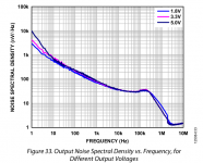
For completeness, Joseph informed me that there was indeed a large difference in the way the reference voltages were generated between the two DACs of which he measured the output signal spectrum. The D90, which had the worst sidebands around the signal, uses ADP7112 references which have lots of subsonic noise that rolls off at roughly 9 dB/octave. It's only 600 nV/sqrt(Hz) at 10 Hz, though, instead of the 6 uV/sqrt(Hz) that I calculated. See the 5 V trace of figure 33 of https://www.analog.com/media/en/technical-documentation/data-sheets/ADP7112.pdf The other DAC used an LT3045.
LT3045 is typical 0.8 uVrms 10Hz to 100KHz, which is 2.5nV/rtHz, while @10Hz is 70nV/rtHz, at least of one order of magnitude better compared to the ADP7112.
Weird choice @Topping... must be price driven, the LT3045 is x5 more expensive.
If I understand your web site, your digital effort is a commercial SACD player.
What????????????????????????????????????????
Right. I hope you are aware that such achievement resides at speaker quality and how they interact with the room, not in digital domain in 21st century.Sorting out the combination that serves one's needs and produces sound that achieves your goal is a skill in and of itself.
There is a simple explanation: Ian makes very little unsubstantiated claims and his projects seem to be based on solid engineering. He implements and optimizes what is in general known to affect the SQ, by indeed occasionally over designing his projects, but seem to know, for example, that the sensitivity of hearing to jitter is in the 100's of ps at best. And when challenged (which I did myself several times) does not claim he was insulted and starts throwing **** in the fan. He responds calm and tries to support his findings. Which may or may not be correct, that's besides the point. If the points are still under contention, he agrees to disagree, and that's it. Ian makes mistakes (like the one with the phase noise measurements using a scope) and I myself did not defend them.
Long story short, Ian doesn't peg the BS meter off scale,
"group buys for profit (self admitted)"
Really?
Never said. I have said several times our target is covering the development costs, no profit here, you are confusing with other threads which have been started for profit.
Often I have lost money with the previous GBs, the last GB has left a little margin I have almost already spent developing the new designs.
So please stop claiming your speculations which have nothing to do with the reality.
"Now please compare with the Andreas approach .... and decide what is/was closer to the DIY spirit"
Really?
- TWTMC-C, Colpitts-Clapp oscillator
- TWTMC-D, Emitter coupled oscillator
- TWTMC-P, Pierce CMOS oscillator
- TWTMC-AIO, Oven for Emitter coupled oscillator with SC-Cut crystal
- TWTMC-D&D, Oscillators power supply, clock switch and dividers
- TWRPS-pp micro, Push-pull low noise regulator
- TWRPS-pp, Push pull low noise voltage regulator
All the schematics and BOMs have been published, just DIY spirit.
- TWTMC-DRIXO, Driscoll oscillator
- TWTMC-EXO, Differential oscillator
- TWTMC-PXO, Pierce oscillator
- TWTMC-PXO-AIO, Pierce All in One oscillator
- TWTMC-DBM, Frequency doubler
- TWRPS-UGL, Linear low noise voltage regulator
- TWSAFB-RPI, Raspberry power supply and isolated I2S
- TWSAFB-TX, LVDS transmitter I2S over HDMI
- TWSAFB-RX, LVDS receiver I2S over HDMI
All the BOMs for semi-finished boards have been published, reverse engineer of the missing parts is very easy for those who are interested to see the full schematics, I have specified the parts not easily recognizable in the thread.
Close enough to the DIY spirit.
So please stop claiming your distorting reality.
"his projects seem to be based on solid engineering"
Really?
Oh yes, our projects are based on incompetence.
2020, August 27th. Fourth picture: "there is crosstalk at SCK clock. Crosstalk should be removed". Just a suggestion in the diy spirit.
Asynchronous I2S FIFO project, an ultimate weapon to fight the jitter
2020, November 13th. "I'm currently working on ReclockPi project".
Asynchronous I2S FIFO project, an ultimate weapon to fight the jitter
2021, April 15th.
ReClockPi was born!
Asynchronous I2S FIFO project, an ultimate weapon to fight the jitter
Someone wrote:
"I have to guess reclockPi fixes some leftover problems from the fifo."
No reply from the designer.
The reclocker of the reclocker, sorry if this looks to me as "solid business" instead of "solid engineering".
I would like to call it the "diy audio philosopher's stone", how to turn a mistake into business.
So please stop with your unsupported engineering comparison, at least until we have made clear and irrefutable mistakes in our designs.
Once and for all, please stop trolling with the only purpose of attack me and my co-developer.
If your target is to get my threads closed or to get me banned you are wasting time.
It does not harm us, in case it harms the members on this forum interested in our projects since in case we will stop designing for the diy audio community.
Fortunately, in case, we could still afford to develop the devices we need for our audio system.
Now I hope this thread get back on topic, such as subharmonics in frequency doublers and higher overtone crystal oscillators.

Nothing more is needed in digital audio as this technology is already audibly transparent. Any further enhancement is for marketing / bragging rights.we could still afford to develop the devices we need for our audio system.
D
Deleted member 537459
D
Deleted member 537459
has anyone found acoustic differences in the sma cables? rg316-rg400 etc.
Yes, this is indeed an appropriate topic in this thread.
D
Deleted member 537459
Part of the title is, "Building a low phase noise/jitter crystal oscillator". Perhaps you don't understand the relevance of audible traits in audio gear. What would help you is to read about the basics of hi-fi audio electronics.@Evenharmonics good idea, read instead of listening and making your own opinion. but please keep reading instead of writing trivial things not relevant to the main speech.
LT3045 is typical 0.8 uVrms 10Hz to 100KHz, which is 2.5nV/rtHz, while @10Hz is 70nV/rtHz, at least of one order of magnitude better compared to the ADP7112.
Weird choice @Topping... must be price driven, the LT3045 is x5 more expensive.
I would guess that the ADP7112 has an internal low-pass filter consisting of a switched-off MOSFET and a capacitor of 100 pF or less or something like that. I don't see how else it can produce such insane amounts of subsonic noise (6 uV/sqrt(Hz) at 1 Hz...). Pity there is still a factor of ten discrepancy between the datasheet noise density at 10 Hz and what I calculated based on Joseph's audio noise sideband measurements. Then again, if my guess is correct it will spread all over the place, and the datasheet has only typical figures.
Anyway, if you want to minimize skirts around the audio signal, use a voltage reference with low noise, also in the subsonic region.
Last edited:
No idea what you mean by "internal low-pass filter consisting of a switched-off MOSFET and a capacitor of 100 pF or less" but I would think the ADP7112 is using a CMOS error amplifier, these are known for having a high noise corner frequency and also some excess 1/f noise (1/f^n) due to the trapping-detrapping carrier fluctuations in the channel.
The ADP7112 series has a few features that make me suspect they have an internal low-pass filter:
1. For the fixed-voltage types, the noise density above 10 Hz is roughly independent of the output voltage, but the noise density at 1 Hz does depend on it.
2. It has a soft-start feature; without any external soft-start capacitor, the voltage settles to 90 % in 380 us (equivalent to a time constant of 165 us)
3. The output noise density of the 5 V version drops from about 10 uV/sqrt(Hz) to 600 nV/sqrt(Hz) between 1 Hz and 10 Hz (that 6 uV/sqrt(Hz) from post #4636 was a mistake, it's 10 uV/sqrt(Hz)). That's much faster than normal excess noise. There is a normal 1/f slope from about 20 Hz to 3 kHz, for all output voltages.
It's only a guess as I never worked for Analog Devices, but it looks to me like they have some high-noise reference, an amplifier that amplifies the reference to the required output voltage depending on the voltage variant, a low-pass filter that can be switched between 165 us time constant at start-up and a huge time constant (> 160 ms) after start-up, and then a voltage follower.
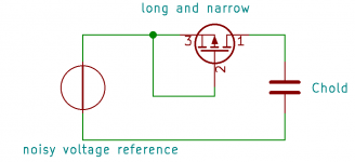
As the ADP7112 can survive 20 V, it is probably made in an old CMOS process where the gate oxide is still thick enough to make gate tunnelling current negligibly small. In that case, a practical way to make an on-chip filter with two time constants would be a basic sample and hold with a long and narrow PMOS switch of which the bulk is connected to the input. Switch it on and you have a 165 us time constant set by the on resistance and the hold capacitor, switch it off and you get the huge time constant needed to suppress 10 Hz noise sufficiently. With the PMOS off, weak inversion conduction of the PMOS and its drain-bulk leakage both tend to keep the voltage at the hold capacitor at the correct value, so as long as they are much greater than the oxide tunnelling current of the capacitor and the output voltage follower, the voltage won't drift away.
1. For the fixed-voltage types, the noise density above 10 Hz is roughly independent of the output voltage, but the noise density at 1 Hz does depend on it.
2. It has a soft-start feature; without any external soft-start capacitor, the voltage settles to 90 % in 380 us (equivalent to a time constant of 165 us)
3. The output noise density of the 5 V version drops from about 10 uV/sqrt(Hz) to 600 nV/sqrt(Hz) between 1 Hz and 10 Hz (that 6 uV/sqrt(Hz) from post #4636 was a mistake, it's 10 uV/sqrt(Hz)). That's much faster than normal excess noise. There is a normal 1/f slope from about 20 Hz to 3 kHz, for all output voltages.
It's only a guess as I never worked for Analog Devices, but it looks to me like they have some high-noise reference, an amplifier that amplifies the reference to the required output voltage depending on the voltage variant, a low-pass filter that can be switched between 165 us time constant at start-up and a huge time constant (> 160 ms) after start-up, and then a voltage follower.
As the ADP7112 can survive 20 V, it is probably made in an old CMOS process where the gate oxide is still thick enough to make gate tunnelling current negligibly small. In that case, a practical way to make an on-chip filter with two time constants would be a basic sample and hold with a long and narrow PMOS switch of which the bulk is connected to the input. Switch it on and you have a 165 us time constant set by the on resistance and the hold capacitor, switch it off and you get the huge time constant needed to suppress 10 Hz noise sufficiently. With the PMOS off, weak inversion conduction of the PMOS and its drain-bulk leakage both tend to keep the voltage at the hold capacitor at the correct value, so as long as they are much greater than the oxide tunnelling current of the capacitor and the output voltage follower, the voltage won't drift away.
Attachments
Last edited:
In that case, a practical way to make an on-chip filter with two time constants would be a basic sample and hold with a long and narrow PMOS switch of which the bulk is connected to the input. Switch it on and you have a 165 us time constant set by the on resistance and the hold capacitor, switch it off and you get the huge time constant needed to suppress 10 Hz noise sufficiently. With the PMOS off, weak inversion conduction of the PMOS and its drain-bulk leakage both tend to keep the voltage at the hold capacitor at the correct value, so as long as they are much greater than the oxide tunnelling current of the capacitor and the output voltage follower, the voltage won't drift away.
I never saw such a switching filter (looks like a ZOH) included in an analog CMOS circuit who does not require a mixed signal process, but I suppose it can be done. I’ve seen regulators that do not require an output capacitor, those do probably have something like this, but for the ADP I don’t know why they would add it, since they specify a 2.2uF or larger at the output. You mean for reference filtering?
BTW, both the sub threshold conduction and the bulk diode leakage of the switch trend to discharge a S&H capacitor, not to keep the voltage constant, not sure why you think otherwise. How long would it take to discharge the cap, if there is no refresh mechanism to control the switch other than the startup? Wouldn’t the output voltage of the regulator decrease in time, as the cap discharges?
Last edited:
Yes, I mean for reference filtering. When you look at the attached schematic, except for capacitor and output buffer (not drawn) oxide tunnelling leakage and as long as it is perfectly dark, leakage and weak inversion currents will tend to pull the voltage across the capacitor in whatever direction reduces the voltage between drain and source and between drain and bulk of the PMOS, which is exactly what is needed. It is essential that tunnelling leakage is much smaller than junction and weak inversion currents and that the noisy reference is kept switched on in hold mode.
By the way, as the capacitor works with a more or less constant charge in it, the ratio between charge and voltage (that is, the capacitance if it is a linear capacitor) needs to be temperature-independent to prevent drift when the junction temperature changes. The PMOS could also be a small PMOS with a large polysilicon resistor in series, at least that keeps the time constant in sampling mode independent of the reference voltage. Like I wrote, I expect the voltage at the input of this hypothetical filter is an amplified reference voltage that depends on what output voltage variant you use.
By the way, as the capacitor works with a more or less constant charge in it, the ratio between charge and voltage (that is, the capacitance if it is a linear capacitor) needs to be temperature-independent to prevent drift when the junction temperature changes. The PMOS could also be a small PMOS with a large polysilicon resistor in series, at least that keeps the time constant in sampling mode independent of the reference voltage. Like I wrote, I expect the voltage at the input of this hypothetical filter is an amplified reference voltage that depends on what output voltage variant you use.
Attachments
Last edited:
- Status
- Not open for further replies.
- Home
- Source & Line
- Digital Line Level
- The Well Tempered Master Clock - Building a low phase noise/jitter crystal oscillator