Most of the time, doing all the work to figure out what numbers you can trust from your equipment and test setup simply depresses you! 🙂
-Chris
So true 😎
Disappointing results on Exar/Sipex samples
The first SPX431 was actually worse than a JRC 431, about 155nV/sq rt Hz in an 80kHz NBW. The noise was insensitive to operating current between 1mA and 10mA.
The SOT-23-3 SPX2431 was somewhat quieter, but still well above the datasheet typical, at about 96nV/sq rt Hz under similar conditions. I could test more but I would repurpose my test socket rather than trying to solder to them, and I don't want to spend the time right now. Another disadvantage of the 2431 is a max cathode voltage of 20V. They are almost certainly different chips than their 431.
However, while searching unsuccessfully for the JRC spec, I noticed that the On Semi part is supposedly quieter than the run-of-the-mill, at about 48nV/sq rt Hz. And it has the advantage of existing in TO-92.
So I will try to get some of those now.
Was it insensitive to operating current when tied as a 2.5V unity gain source? Or you also tried with a couple of resistors to make it give say 5-20V? The old reports were saying that it was not changing noise when just strapped to unity but 1mA was better when there was operating current bias variance if in higher than its own ref voltage.
Was it insensitive to operating current when tied as a 2.5V unity gain source? Or you also tried with a couple of resistors to make it give say 5-20V? The old reports were saying that it was not changing noise when just strapped to unity but 1mA was better when there was operating current bias variance if in higher than its own ref voltage.
Just cathode to reference for 2.5V. This is also the configuration shown for specifying noise. No capacitor other that maybe the 1nF of the Ap cable and input capacitance.
When its handy again give it a try if you will remember. Using it solely as a 2.5V ref rather unlikely. But boosted in voltage surely. Noisier samples than in the old times? It had a 50nV reputation. As through hole part.
Hi Brad,
That's very good to know. I am encouraged that the On-Semi part is supposed to be less noisy. On-Semi parts have been pretty good.
I would be extremely interested in the results when running the 431 with voltage gain. It may get noisier, but if that is slight then the part has more latitude for designs. Maybe there is a sweet spot for noise at some voltage.
I haven't got a setup where I can measure noise like you can, otherwise it would be something I could do.
-Chris
Stacking a bunch of them as I've done is where the 2.5V is convenient, although I did do a measurement some time ago to see how much the use of gain affected the noise. It was of course worse than simply the voltage gain + 1 times the noise at 2.5V. I have forgotten what the impedance of the divider was. I usually put 1mA through it, hence the divider R 2.49k.When its handy again give it a try if you will remember. Using it solely as a 2.5V ref rather unlikely. But boosted in voltage surely. Noisier samples than in the old times? It had a 50nV reputation. As through hole part.
But it wasn't horribly worse. Notes are around somewhere.
I have had good luck with On Semi (and before that, with Motorola).Hi Brad,
That's very good to know. I am encouraged that the On-Semi part is supposed to be less noisy. On-Semi parts have been pretty good.
I would be extremely interested in the results when running the 431 with voltage gain. It may get noisier, but if that is slight then the part has more latitude for designs. Maybe there is a sweet spot for noise at some voltage.
I haven't got a setup where I can measure noise like you can, otherwise it would be something I could do.
-Chris
Hi Preamp,
No, it isn't a low noise solution, but it is how you would set up a tracking power supply with bipolar output polarities. You can also extend this idea to make the output voltages different, like + 10 V and - 5 V if you needed that.
For low noise applications, you would use what Salas has designed, or something very similar. The noise output of the reference voltage will affect the overall noise fairly directly.
-Chris
For the circuit I'm talking about, the "master" supply is the only one that uses a zener reference. The tracking supply follows the master by sensing changes in a balance point. Simplified then. One supply works as you would normally set a regulated supply up. Then we take a pair of equal resistors (say 10 K) in series between the first regulated supply, and the other supply output. The junction of those resistors will be zero V if both supplies have an equal but opposite magnitude output. Call it + 10V and - 10V. The slave regulator senses the difference between the junction of the two 10 K resistors and the common ground. The slave regulator must change it's output voltage to maintain the 0 V level. This works very well and the circuit is in common use.I'd say no, the voltages don't track each other, as each rail has it's own Zener reference for voltage.
No, it isn't a low noise solution, but it is how you would set up a tracking power supply with bipolar output polarities. You can also extend this idea to make the output voltages different, like + 10 V and - 5 V if you needed that.
For low noise applications, you would use what Salas has designed, or something very similar. The noise output of the reference voltage will affect the overall noise fairly directly.
-Chris
For the circuit I'm talking about, the "master" supply is the only one that uses a zener reference.
That's right and true, but I thought Paul was referring to "my" Dual Salas version, which is not tracking and hence does not work like the circuit you were talking about. Maybe it's just me who didn't get that in the first place 😱.
OnSemi has 3 different 431 variants that I can see, one of them has potentially competitive noise, assuming they are not shameless liars.
http://www.onsemi.com/pub_link/Collateral/TLV431A-D.PDF
http://www.onsemi.com/pub_link/Collateral/TL431-D.PDF
http://www.onsemi.com/pub_link/Collateral/NCP431-D.PDF
http://www.onsemi.com/pub_link/Collateral/TLV431A-D.PDF
http://www.onsemi.com/pub_link/Collateral/TL431-D.PDF
http://www.onsemi.com/pub_link/Collateral/NCP431-D.PDF
OnSemi has 3 different 431 variants that I can see, one of them has potentially competitive noise, assuming they are not shameless liars.
http://www.onsemi.com/pub_link/Collateral/TLV431A-D.PDF
http://www.onsemi.com/pub_link/Collateral/TL431-D.PDF
http://www.onsemi.com/pub_link/Collateral/NCP431-D.PDF
Yes, just the TL431 is interesting.
Hi Preamp,
Hopefully everything is more clear now.
Naw. If I confused you, there were most likely others in the same boat.Maybe it's just me who didn't get that in the first place
Hopefully everything is more clear now.
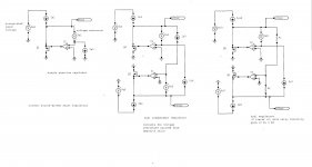
types of shunt regulators
Just to clarify, here are simplified schematics of the sorts of shunt regulators we've been discussing.
The first single one is the basic design of the thread. The error amp triangle is not specifically an op amp.
The second is an independently-referenced dual regulator showing the currents for the voltage references derived from the opposite rails, following Preamp.
The third is the use of the positive regulator output as the reference voltage for the negative rail, hence tracking the magnitude of the changes (if any) in the positive regulator. Of course it could be the other way around, with the negative regulator the primary and the positive derived from the negative.
The fourth shows the reference voltages being generated from the current sources, independently. The resistors developing the voltages will be bypassed with capacitors.
The fifth shows the positive regulator with the voltage reference developed by a current source driving R5, and the negative regulator derived from the positive regulator output.
All of the regulators benefit from low noise gain with respect to the error amps, unlike many other topologies. Even the ones with the opposing rail referencing the other can have very low noise gain if the resistors R2 in the third schematic and R2 in the fifth schematic are well-bypassed.
Attachments
Hi Brad,
Nicely packaged. This shows the different types well, and their differences.
Brad, Salas, (or anyone else) ...
One thing that I know must confuse some people is the concept of noise gain, as opposed to the gain of a stage, like a voltage amp in this case. Care to give that a whirl?
-Chris
Nicely packaged. This shows the different types well, and their differences.
Brad, Salas, (or anyone else) ...
One thing that I know must confuse some people is the concept of noise gain, as opposed to the gain of a stage, like a voltage amp in this case. Care to give that a whirl?
-Chris
Noise gain is the difference left between the gain level you actually want to set and the unity gain level in an open loop gain plot I think.
Yes but like in gain bandwidth product plotting
P.S.
So as the noise gain level meets GBW phase you can see the stability margin you got down to the minimum possibly stable gain over useful area between unity gain and noise gain levels.
P.S.
So as the noise gain level meets GBW phase you can see the stability margin you got down to the minimum possibly stable gain over useful area between unity gain and noise gain levels.
Hi,
In it's simplest form, noise gain is simply the gain of a non-inverting amplifier configuration. Put another way, if β=feedback path attenuation, then the noise gain is 1/β in a non-inverting configuration. If you have an inverting configuration, the noise gain is still what it would be in a non-inverting configuration while your signal gain would be the amount in the inverting configuration.
So for a non-inverting configuration, noise gain = signal gain [Av= (RF /RG) + 1]. For an inverting configuration, noise gain is not equal to the signal gain. Signal gain = |RF/RG|.
I'm going to stop before I confuse the issue more. Can someone explain this a little more clearly than I have please?
-Chris
- Status
- Not open for further replies.
- Home
- Amplifiers
- Power Supplies
- The simplistic Salas low voltage shunt regulator