I read that MPSH81 (PNP) is to replace BC560C (PNP) in v1. This is for the neg rail. What is to replace BC550C (NPN) for the pos rail?
I am not recommending changing v1.
I will be building both. Iko, thanks for posting those schematics and simulating v2 for me. They are for 15.7V rails. I am using SOIC opa627s on browndogs and even the top one runs a bit hot on +/-15VDC and I can imagine the one soldered underneath the browndog may get less heat dissipation. So for +/-15VDC rails I prefer to go under instead of higher. I think I can use exactly the same schematics and component values you posted, only with the 1n4744 replaced with 1n4743 (v1), and 1n4737 replaced with 1n4736, to get about 13.6V instead of 15.7V, to reduce the heat on the opa627 for some peace of mind. Have you got an existing PCB design for v2? If not, I could use ExpressBCP to draw one in reference to the PCB layout of the existing v1.
Thanks,
Bill
That's right, all you need to change is the zener value to go a bit lower. As far as pcb goes, I built all my prototypes without a pcb. I'm working on one, but it's not finished yet.
what are irfbc40?For v2:
IRFBC40LC => No IRFBC40LC available, ............
mpsh81 => Found mpsh81"D27Z
and mpsh81?
what are irfbc40?
and mpsh81?
These are for a version I posted a few pages back.
Edit: here you go Andrew, post 1168
http://www.diyaudio.com/forums/showthread.php?p=1940607
Last edited:
Move the voltage trimmer in line with the Vref leds instead having it under the driver BJT. Unless you only trim it for hitting 5V exactly. It squeezes the margin across the error loop components a lot in a low voltage near Vgs application.
I would suggest to use trimmers only while prototyping. Then measure the value and replace the trimmer with a fixed resistor. I've measured all kinds of noise from some trimmers.
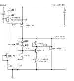
+5V adjustable V1 🙂
You can se here:
http://www.diyaudio.com/forums/showthread.php?t=143693&page=122
i use Salas shunt for my DAC.
it very best, i likes it!
@salas
read back to page 80 🙂
Regulators are used as power supply for DAC and as power supply for Squeezebox & some experiments as power supply for SPDIF circuits and other digital stuff
In all circuits shunt reg is doing very good job 🙂 Thanks to you & Ikoflexer
read back to page 80 🙂
Regulators are used as power supply for DAC and as power supply for Squeezebox & some experiments as power supply for SPDIF circuits and other digital stuff
In all circuits shunt reg is doing very good job 🙂 Thanks to you & Ikoflexer
There have been a number of PCB designs published in this thread. I would be happy to use any of them if I had them on hands. Since I always use dot matrix type of veroboard and solder components point to point, I need to design it using ExpressPCB so that I know exactly which dots I should put the component leds on.
So here it is:
So here it is:
An externally hosted image should be here but it was not working when we last tested it.
With the above drawing, note that:
a) I could not find the symbol for TO-247 so I simply used TO-220. I have reserved sufficient space for TO-247.
b) There should be sufficient space for paralleling up to 4 x 2W-3W metal film resistor for R1 (in place of the 15R resistor). Wirewound resistor has higher inductance and can not be used here. For lower resistor value (higher current), say for a given voltage 10R x 0.5A x 0.5A = 2.5W, we need at least 2 x 2W resistor in parallel or series. I personally would go at least 4 times for component rating.
c) I could make the path, especially the path between the MOSFETs shorter by using different orientation of the MOSFETs, but in that case I can not use one piece of large heatsink for the MOSFETs for higher current application. The design above allows using individual small heatsink for each MOSFET, or one large piece of heatsink, or aluminium flat/angle/U, etc.
I had these in my mind:
d) Move the last C in the raw DC supply to this board. This will provide a shorter AC current loop. I would imagine that the shuntreg board would be closer to the load board, and the raw DC board would be closer to the transformer. Since the load board should be as far away from the transformer, the distance of the raw DC and the shuntreg can be long. Therefore, I have the space for 0.1uF || 2,200uF on this board.
e) The current paths are made as short, straight as possible to reduce wire resistance and inductance.
f) All gate resistors are place close to the gates.
g) The sensing point (D1, C2) is right at the output.
h) Star ground for the shunt.
i) Thick and (as straight as possible) wires to be used for the main DC and AC current loops.
j) Capacitors are at reasonable distance away from the heatsinks, as heat will shorten capacitors' lifes.
Please let me know what you think and point out any errors, shortcomings and suggest improvements. I am keen to learn. The drawing is not finalised yet. It was a piece of work of about 6 hours today.
Regards,
Bill
Last edited:
All the above are positive moves, and P2P is great. I do it all the time. Looks like a good scheme. I did not look thoroughly in your layout though. Good luck.
Did it get to improve with use and / or MPSA18?
Very difficult to make direct & fair comparision BC550 vs. MPSA18. Soldering/desoldering take time & sonic impression get lost. By my humble personal opinion MPSA18 is better.
More audible is capacitor C2 (see post #745).
I like there big value film capacitor, not lytic. Or lytic bypassed with film. Value depends on personal preferences, between 2.2uF and 2200uF
Thanks. You probably could say a bypass ratio between 1/1000-1/100? Also when sinking is good, the heavier it runs, the better, but depends on the circuit it serves. Some show more, some not.
I dont think ratio is important. Value & quality is more important.
Lower value = less bass, more highs, some harshness in highs, better dynamic
Bigger value = more bass, less highs, silky smooth highs, less dynamic
Lower value = less bass, more highs, some harshness in highs, better dynamic
Bigger value = more bass, less highs, silky smooth highs, less dynamic
Last edited:
Very difficult to make direct & fair comparision BC550 vs. MPSA18. Soldering/desoldering take time & sonic impression get lost. By my humble personal opinion MPSA18 is better.
More audible is capacitor C2 (see post #745).
I like there big value film capacitor, not lytic. Or lytic bypassed with film. Value depends on personal preferences, between 2.2uF and 2200uF
Big value film caps become costly - this cap flavouring was something I was hoping to avoid both on a cost basis and time & peace of mind basis 🙂
Have you tried a motor run capacitor in this position? I believe these are polypropylene but bulky - maybe bypassed with a higher quality polypro?
One of the signs of a good regulator, I've heard, is that the quality of the PS feeding into it (within reason) becomes immaterial. Does this apply here - is there a sonic difference when different caps are used in the PS feeding this reg?
- Status
- Not open for further replies.
- Home
- Amplifiers
- Power Supplies
- The simplistic Salas low voltage shunt regulator