Now look at the effective impedance of the CCS.I tried the experiment for that same -0.47V Vp K170BL. A jumper between G & S. A variable PSU for VDS. The thick red lead in the picture goes to a Fluke 87V in series mA DC mode for better readings than the PSU's at this difficult for its resolution region.
VDS / Id
10V 7.20mA
4.0V 6.93mA
1.0V 6.39mA (at about 2*Vp)
0.7V 6.17mA (at about Vbe)
0.5V 5.83mA (at about 1*Vp)
0.3V 4.84mA
So 9.6% current fall between 2*Vp and 1*Vp at Vgs=0
using each adjacent pair of voltage & current to calculate the average slope of the Id vs Vds I get
10V to 4V gives 25k9
4V to 1V gives 5k6
1V to 0V7 gives 1k4
0V7 to 0V5 gives 0k59
0V5 to 0V3 gives 0k20
An excellent CCS has an effective impedance that approaches infinity, i.e. the slope of the Id vs Vds plot is flat.
good CCS are probably in excess of 100k.
A jFET with a low Vds is showing effective impedances of <26k to ~200ohms.
As I said a few posts back, the CCS with too low a Vds behaves as a low value resistor.
Any of our Members can repeat the experiment and compare the effective impedance of their jFET CCS @ a Vds= 2Vp and @ a Vds =1.5Vp and @ Vds=Vp
Their results will show that the CCS needs a higher Vds voltage than Vp
Use Borbely's Vds>2Vp, to get the jFET into an operating region where it possesses some CCS character.
Why is all this being discussed?
Because the current through the voltage reference resistor must be held constant. If the voltage reference changes then the output voltage changes. An unchanging voltage reference gives a more constant output voltage. If there are small changes in output voltage, then that is the same as noise. The better the CCS, the lower the output noise. This can be low frequency noise and middle frequency noise and high frequency noise.
Addendum:
select your test voltages.
now measure the current when the Vds is testvoltage+10mV and again for testvoltage-10mV. Plot the two results and calculate the average SLOPE across the testvoltage.
Last edited:
The deeper operated in the saturation region the stiffer no doubt. When looking at the brown 0 Vgs trace in #6831 we see that 0.9V (~2Vp) still does not clear the Ohmic region's shallow portion. So the 2Vp rule of thumb is still a border guideline. If interpreted as a guideline to surely stay out of the steep Ohmic portion, then 2Vp in the sense of numbers distance ref zero still does that in those curves. A source resistor to provide 0.17V Vgs looks like flattening out the curve better even when at Vbe for VDS (magenta).
Addendum:
select your test voltages.
now measure the current when the Vds is testvoltage+10mV and again for testvoltage-10mV. Plot the two results and calculate the average SLOPE across the testvoltage.
This time for a 0.6V Vp K117
VDS / Id
10V 5.69mA
4V 5.52mA (35k from 10V)
1.2V 5.17mA (2Vp)
1V 5.08mA (6.81k from 4V)
0.6V 4.63mA (Vp)
Fine step in the variable PSU:
1.2V 5.163mA
1.19V 5.160mA
(2Vp region 3.33k)
0.7V 4.811mA
0.69V 4.795mA
(Vbe region 0.625k)
0.6V 4.629mA
0.59V 4.607mA
(|Vp| region 0.454k)
Conclusion is that the K117 shows somewhat better CCS due to different output conductance than K170. When still comparable for noise spec. Also using a low side GR circa 3mA Idss (the sample was high side GR) will be stiffer still when just under Vbe. As done in V1.1 BIB. So the 2Vp rule of thumb works stronger in lower Yfs JFETS of higher Vp. When 2Vp taken as an absolute number |Vp| always keeps away from the steepest Ohmic region portion in any type of JFET.
K117GR 3.15mA Idss -0.47V Vp
1.00V 2.738mA
0.99V 2.735mA
0.70V 2.635mA
0.69V 2.630mA
0.50V 2.487mA
0.49V 2.477mA
3.33k - 2k - 1k
1.00V 2.738mA
0.99V 2.735mA
0.70V 2.635mA
0.69V 2.630mA
0.50V 2.487mA
0.49V 2.477mA
3.33k - 2k - 1k
The design does do well on noise, and low output impedance, but clearly among the typical specifications for a regulator will be accuracy (for which we have an adjustment) and temperature stability, for which we have to pretty much take what we can get. It's interesting that the short-channel JFETs like the SK170 and SK117 (the latter essentially a half-gate-width 170) have a positive tempco of drain current even at Idss. If you slightly forward-bias the gate-source the tempco can be adjusted to about zero, and I find this happens well before there is significant forward gate current. There will be a small effect from the input transistor's base-emitter voltage tempco, although this will become more important if the current sink device is low impedance, and at the point that the 47k and current sink looks like just a voltage divider, the regulation ceases.Why is all this being discussed?
Because the current through the voltage reference resistor must be held constant. If the voltage reference changes then the output voltage changes. An unchanging voltage reference gives a more constant output voltage.
I've used the basic arrangement of current source and shunt regulator several times before, most recently for a MC stepup stage that was relatively simple but very demanding of the power supplies (I was catering to the no-global-feedback and simpler-is-better crowd in this case). The shunt reg was a fairly straightforward bipolar arrangement, with an NMOS power device as the shunting element, and the reference determining the output voltage was a few paralleled JFETs I had a whole ammo box of, for which I adjusted a common source resistor to get to the zero tempco operating point.
The nice thing about the Salas reg is the low noise gain, due to the 47k shunted by the big cap acting as a R-C feedback resistor. Note that Linear Tech has recently touted a new LDO with the claim to fame of lower noise due to a somewhat similar approach (departing from the typical lower voltage reference), with an internally-generated current developing a voltage across an external resistor, and essentially a unity-gain amplifier (however they don't reveal how they make the internal current source quiet, although the developed voltage can be readily filtered with an external cap).
The nested JFET in the SSLV regs does not get shook by a strongly changing VDS. Vbe is its VDS that follows only very slightly the error amp action. It could be a 250R instead with the PSRR & Zo of the total circuit hardly changing. But a low side Vp JFET is still 8 times better for sourcing the same current to the Vref. If better tempco and about same noise spec any low enough Vp type does the trick. Or just a resistor if not having any. Won't spoil the soup that much.
No, and for many applications it will be fine. It is nonetheless true that temperature stability may be a more critical parameter for certain applications. Both low noise and low tempco can be achieved mutually.The nested JFET in the SSLV regs does not get shook by a strongly changing VDS. Vbe is its VDS that follows only very slightly the error amp action. It could be a 250R instead with the PSRR & Zo of the total circuit hardly changing. But a low side Vp JFET is still 8 times better for sourcing the same current to the Vref. If better tempco and about same noise spec any low enough Vp type does the trick. Or just a resistor if not having any. Won't spoil the soup that much.
Yes, those will work but also have a large temperature coefficient.We use a string of Leds instead of a Norton Vref in case we want a stiffer Vref. See DCB1.
BTW---does the last posted regulator schematic have a starting problem? I conjectured, looking at it, that it might, and simulations seem to confirm that.
Brad
Not sure, but I saved it:In which #post?
Attachments
I remember that the 1.2 Version (which has the same cascode tail CCS governed by 1 Vbe/R current set as the V1.2R) prototype (green matrix board) needed a compact layout for the whole CCS portion of the reg not to fail starting. http://www.diyaudio.com/forums/powe...-voltage-shunt-regulator-190.html#post2103488
That's because the tail end of the CCS is fed from the regulated line for very good PSRR. Thus it won't accept additional lag due to makeshift layout.
That's because the tail end of the CCS is fed from the regulated line for very good PSRR. Thus it won't accept additional lag due to makeshift layout.
You see the issue though? I can't believe it pertains to delay in a layout. In the others the JFETs pull current immediately, which then turns on the PMOS until the Vbe of the local transistor Q2 turns on to limit the current. With the bipolars and LED, fed from the +35V output, once up it works fine. But otherwise the bipolars don't turn on without something to bring up the +35V output at least a little, or something to turn on Q3 and Q4. You could provide a voltage divider from the +45V that goes to the base of Q3 through a diode, which then as the +35V comes up, gets reversed-biased and therefore out of the circuit, and get your advantage of improved PSRR. It should only take a few volts, although the impedance of the added divider will need to account for the loading of the 3.3k's.I remember that the 1.2 Version (which has the same cascode tail CCS governed by 1 Vbe/R current set as the V1.2R) prototype (green matrix board) needed a compact layout for the whole CCS portion of the reg not to fail starting. http://www.diyaudio.com/forums/powe...-voltage-shunt-regulator-190.html#post2103488
That's because the tail end of the CCS is fed from the regulated line for very good PSRR. Thus it won't accept additional lag due to makeshift layout.
This is an issue endemic to various bootstrapped arrangements.
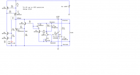
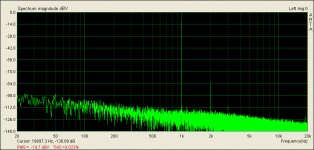
Here is a later photo I just found of how it got closer together. Never ever missing a start up. Since that was converted to 1.2R also and we had its noise analysis discussed you can see an FFT (1V=0dB) of an FSP (Folded cascode input stage single ended no loop feedback JFET phono at LMC 63dB gain) it powers (one PSU for both channels).
Attachments

You see the issue though? I can't believe it pertains to delay in a layout. In the others the JFETs pull current immediately, which then turns on the PMOS until the Vbe of the local transistor Q2 turns on to limit the current. With the bipolars and LED, fed from the +35V output, once up it works fine. But otherwise the bipolars don't turn on without something to bring up the +35V output at least a little, or something to turn on Q3 and Q4. You could provide a voltage divider from the +45V that goes to the base of Q3 through a diode, which then as the +35V comes up, gets reversed-biased and therefore out of the circuit, and get your advantage of improved PSRR. It should only take a few volts, although the impedance of the added divider will need to account for the loading of the 3.3k's.
This is an issue endemic to various bootstrapped arrangements.
There was something like that we had done with a diode also back then, or a zener, can't remember exactly how now, but interestingly when I brought everything input CCS very close together it never failed to start again in the prototype. Still works in that phono build.
P.S. If it was a finalized thing for general builds on a proper PCB it would need some sure start mechanism to avoid any chance of stalling of course.
P.S. If it was a finalized thing for general builds on a proper PCB it would need some sure start mechanism to avoid any chance of stalling of course.
Further reflection and modeling, I see how it comes up now: with the shunt section low, thus no bias on the voltage divider and LED, the transistors in the current source still have collector leakage (my model says something in the vicinity of 50pA). Only if the PNP has a good deal larger amount (unlikely, particularly at an initial low voltage) will it dominate the determination of the voltage at the gate of the PMOS, and have it be a small magnitude gate-source voltage, thus keeping it off. But almost surely the NPN leakage and the PNP leakage will start to reach an equilibrium at that junction of collectors and PMOS gate, which will also, almost surely, be a larger magnitude than the required gate-source PMOS threshold. So PMOS will turn on, and then everything comes up. Initially, for a short time the shunt regulator output sits at around 3V while the 4.7uF feedback cap charges, but then the shunt reg voltage ramps up to the desired output voltage.
Good explanation. There was a faint glimpse of light in the CCS Led when the layout was wider and once in a few power ups it did not start but a touch with a DMM probe to Q1 could kickstart it.
😎
😎Good explanation. There was a faint glimpse of light in the CCS Led when the layout was wider and once in a few power ups it did not start but a touch with a DMM probe to Q1 could kickstart it.
- Status
- Not open for further replies.
- Home
- Amplifiers
- Power Supplies
- The simplistic Salas low voltage shunt regulator