Q5 (jFET) attached to Q3 (bjt) must be a 2sk170gr or lsk170a
A 6mA idss device operating with ~600mVds will pass ~4mA as a CCS current.
A 6mA idss device operating with ~600mVds will pass ~4mA as a CCS current.
Version 2 in all its fictitious glory is here for perusal, checking, comments, and corrections. Totally untested too, ugly, and looking for a loving house. Who's first, who's first?
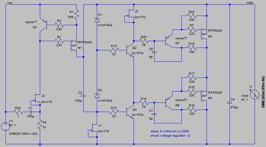
A few comments on the circuit, and these are according to my simulations.
1) The shunt mosfets current and power dissipation with 1mA load:
R1 = 2R8 I = 412mA P_M2 = 2.9W P_M3 = 7.2W
R1 = 3R3 I = 346mA
R1 = 4R5 I = 246mA
R1 = 6R8 I = 153mA P_M2 = 1.2W P_M3 = 2.7W
2) The components shown seem to do best in simulation, but other parts may do the job with a slight decrease in performance. The darlingtons MPSA77 are easy to find and dirt cheap. However, you can use BC560C in this position as well. Instead of the BC107A anything with a lowish hfe should be ok, such as 2N3904, BC550B, etc.
3) All of the jfets in the simulation were set in the range of 7 to 8 mA Idss.
4) C7 and C8 are needed to stop oscillation. The actual value in real life may have to be a little higher (up to 100pF) or they might not be needed at all.
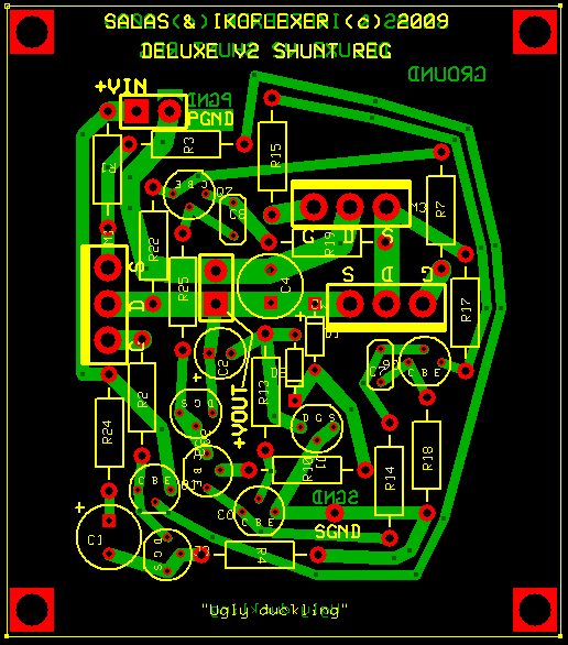
A few comments about the pcb. It looks like a huge mess right? Yes, it does. The underlying theme was "high frequency." Whether that's even needed, its questionable, but I wanted it so. The few rules I tried to abide to were:
a) the signal trace should be non-inductive as possible, meaning short, on the thick side, and straight; for us these are the segments between
b) M1 should be mounted on top, no need for a huge sink, since it does not need to dissipate lots of heat; M2 and M3 are mounted parallel to the board, underneath; I'm thinking this is a standing pcb. Nobody's perfect.
Enjoy!
http://www.cs.toronto.edu/~relu/audio/regs/reg-salasiko-v2-pcb.pdf
http://www.cs.toronto.edu/~relu/audio/regs/reg-salasiko-v2-silk.pdf
A few comments on the circuit, and these are according to my simulations.
1) The shunt mosfets current and power dissipation with 1mA load:
R1 = 2R8 I = 412mA P_M2 = 2.9W P_M3 = 7.2W
R1 = 3R3 I = 346mA
R1 = 4R5 I = 246mA
R1 = 6R8 I = 153mA P_M2 = 1.2W P_M3 = 2.7W
2) The components shown seem to do best in simulation, but other parts may do the job with a slight decrease in performance. The darlingtons MPSA77 are easy to find and dirt cheap. However, you can use BC560C in this position as well. Instead of the BC107A anything with a lowish hfe should be ok, such as 2N3904, BC550B, etc.
3) All of the jfets in the simulation were set in the range of 7 to 8 mA Idss.
4) C7 and C8 are needed to stop oscillation. The actual value in real life may have to be a little higher (up to 100pF) or they might not be needed at all.
A few comments about the pcb. It looks like a huge mess right? Yes, it does. The underlying theme was "high frequency." Whether that's even needed, its questionable, but I wanted it so. The few rules I tried to abide to were:
a) the signal trace should be non-inductive as possible, meaning short, on the thick side, and straight; for us these are the segments between
b) M1 should be mounted on top, no need for a huge sink, since it does not need to dissipate lots of heat; M2 and M3 are mounted parallel to the board, underneath; I'm thinking this is a standing pcb. Nobody's perfect.
Enjoy!
http://www.cs.toronto.edu/~relu/audio/regs/reg-salasiko-v2-pcb.pdf
http://www.cs.toronto.edu/~relu/audio/regs/reg-salasiko-v2-silk.pdf
if the output is shorted all the power that was dissipated in the Shunt is transferred to M1.
It needs a heatsink.
It needs a heatsink.
Thanks guys. OK, so M1 needs a large heat sink too, and there is room for it. M1 can also be mounted on the back, together with the other two mosfets, possibly on the same large heat sink.
I replaced the ground plane with power and signal ground, PGND and SGND.
I replaced the ground plane with power and signal ground, PGND and SGND.
This is not that far away in concept as it may first look from V1. ''Totem V1 with buffered Darlington drive'', is the short description. Iko will test it in reality, if it all works steady, and there is tangible subjective performance boost, then we will recommend it, not as simplistic anymore, but ''Deluxe V2''. Needless to say that the simulated performance is just fantastic for the parts count. If losing as much as V1 loses from sim in practice, it still must make a difference. We hope its gonna work with no problems, fingers crossed. Darlington hfe can be rebelious you see (but we can always revert to just PNP). OK with that policy Iko?😎
Salas said:Darlington hfe can be rebelious you see (but we can always revert to just PNP). OK with that policy Iko?😎
Right on! Yes, I have my reservations about the darlingtons too, but we reach for the rainbow and if we end up touching the ceiling, it's not a tragedy 😀 No guts, no glory, right?
Start your engines gentlemen, the pcb is taking a bath in etchant right now...
Teddy Pardo found that what went in front of an ALW Jung super regulator (ie the pre-regulator) had a very significant effect on the performance (significant audible effect).
I am not sure that what he has done is entirely relevant to this design, I just want to make sure we cover all bases (it is an interesting read at least) http://www.pinkfishmedia.net/forum/...ead.php?t=29501
So I don't think we should neglect this area, considering the great work that has gone into this so far (unless this design is immune to front end performance).
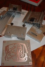
Are you going to solder the Mosfets copper side, bend them legs and mount on sink?
175mA sounds OK. Is that for my MM phono with cascode 1st stage?
P.S. Ah no. The Darlington has more Vbe. So it must be around 0.5A? Why so much?
175mA sounds OK. Is that for my MM phono with cascode 1st stage?
P.S. Ah no. The Darlington has more Vbe. So it must be around 0.5A? Why so much?
I was going to hook-up a 250ohm resistor on the output, and with the 4R R1 it looks like about 200mA through the shunt mosfets.
thanh1973 said:Teddy Pardo found that what went in front of an ALW Jung super regulator (ie the pre-regulator) had a very significant effect on the performance (significant audible effect).
I am not sure that what he has done is entirely relevant to this design, I just want to make sure we cover all bases (it is an interesting read at least) http://www.pinkfishmedia.net/forum/...ead.php?t=29501
So I don't think we should neglect this area, considering the great work that has gone into this so far (unless this design is immune to front end performance).
The link doesn't work.
ikoflexer said:I was going to hook-up a 250ohm resistor on the output, and with the 4R R1 it looks like about 200mA through the shunt mosfets.
I saw 2V Vbe for MPSA77 and that gives roughly 0.5A with a 4R. Anyway, keep 200mA as practical target. You can always measure Vdrop on R1 and change it accordingly.
Salas said:
I saw 2V Vbe for MPSA77 and that gives roughly 0.5A with a 4R. Anyway, keep 200mA as practical target. You can always measure Vdrop on R1 and change it accordingly.
Yes, I saw that too. This does not agree with the simulation. Hm...
If the models are fictional...keep a fire extinguisher handy. Naah, just a bit of suspense. Like in LOST. We gonna see aliens there in the end.. Jacob said ''they are coming'' before he got tossed in the fire by the loophole impostor.
P.S. Congrats to Canada for E. Lilly.😀
Naah, just a bit of suspense. Like in LOST. We gonna see aliens there in the end.. Jacob said ''they are coming'' before he got tossed in the fire by the loophole impostor. P.S. Congrats to Canada for E. Lilly.😀
- Status
- Not open for further replies.
- Home
- Amplifiers
- Power Supplies
- The simplistic Salas low voltage shunt regulator