Top side means the side on top, where the components are.
There is a via (a copper pad used to connect layers on the PCB) between R21 and the gain switch. It is possible for the gain switch leg to contact that via on the top side of the board, causing right channel distortion.
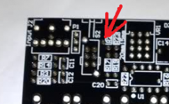
Here's a picture of the corner of the board, where the input jack is. The arrow points to the via, beside R21.
There is a via (a copper pad used to connect layers on the PCB) between R21 and the gain switch. It is possible for the gain switch leg to contact that via on the top side of the board, causing right channel distortion.
Here's a picture of the corner of the board, where the input jack is. The arrow points to the via, beside R21.
Attachments
jep, me mean the same thing. I'm very sure it's not touching, having just jabbed a screwdriver between the 2 points on the circuitboard, removing the leg. still no change in sound.
edit: also another thing: When there is only sound coming from the left channel (right channel disconnected at source) there is a really faint but clean sound on the headphones. Maybe thats important to know
t
edit: also another thing: When there is only sound coming from the left channel (right channel disconnected at source) there is a really faint but clean sound on the headphones. Maybe thats important to know
t
Last edited:
If I have this right... the unit worked on both channels, then only one channel, then switched channels with the op amps, then returned to the original fault. I'm afraid you're back to visual inspection, ohmmeter checks and voltmeter checks as specified in the docs.
yes, you're right. although it could be that I made a mistake on the side switch as I was very tied; this seems more and more likely. That said, I guess I'll have to do the checks with the voltmeter again. thanks so far!
Allright, i've done all the Tests and havn't had any values that werent good. I have no clue how to proceed now. Is there any other testing i could do?
If it were me i would connect a multimeter to the input cable left channel and start checking for continuity along the chain, input jack, R7/R3, opamp input pins (5or3), then output pins (1or7) volume pot etc. Basically following the circuit diagram. It could be something silly like a faulty input jack, volume pot, gain switch etc. Its not uncommon for things to get nuked while soldering.
Thanks for your reply. Sadly, I'm quite unexpirienced in reading circuit bords. Could you tell me the way I need to go through to check the right channel? thankyou very much!
Let me get this right, you have the left channel playing as normal, just no sound on the right?
Also just seen your using an ODAC too, can you post pics of the wiring at each end?
Also just seen your using an ODAC too, can you post pics of the wiring at each end?
Ive uploaded some pictures here:Let me get this right, you have the left channel playing as normal, just no sound on the right?
Also just seen your using an ODAC too, can you post pics of the wiring at each end?
imgur: the simple image sharerimgur: the simple image sharerimgur: the simple image sharerimgur: the simple image sharer And yes, I don't have sound on the right channel, the left one is working fine. No distortion on it, it sounds as expected.
Last edited:
Ive uploaded some pictures here:
Post a picture of the underside of your input jack. I'll bet you didn't fully cut one of the middle traces, like swalter posted.
You don't need those two shorting bars between the outer holes of the input jack and the inner holes. Those inner holes are grounded so that the switch inside the O2's input jack cuts off (grounds) the inputs when nothing is plugged in. The way you have it, if you haven't fully cut those two traces underneath, you will short out your inputs.
You can just remove those two shorting bars entirely and put your wires only in the outer holes of the input jack, then it won't matter if the traces are cut. JDS had that trace cutting stuff in there assuming the O2's input jack was still soldered on. Even better, use those P1 connector holes next to it. The middle hole is ground, the top one (square pad) is left, and the bottom one is right. But you still need to unsolder and remove those two shorting bars. They would short out the inputs through P1, too.
Also make sure that you only cut the traces circled in red below. If you cut anything else you cut an input signal trace.
Attachments


Last edited:
As so: http://i.imgur.com/xQWA3O5.jpg ? I'm sure I've only cut the 2 Ground trace Signals. Is the board multi-layered? Is there another copper wire running "under" the ground wires? I cut pretty deep, so maybe I cought the other wires (if they even exist)?
Much better. 🙂 Now it won't matter if the traces are fully cut or not. The board is just double-sided so you didn't cut anything in the middle. If your problem remains it must be something else.
A couple of photos of the underside would still be a good idea so the folks here can take a look at your solder joints.
Last edited:
I agree with agdr, that looks much better 🙂
You did not tell us if this has fixed your problem though...
In case you still have issues or get stuck you can drop by my workshop at the weekend and we can have a look (and fix it) together.
Drop me a mail or PM for the address.
Stefan
You did not tell us if this has fixed your problem though...
In case you still have issues or get stuck you can drop by my workshop at the weekend and we can have a look (and fix it) together.
Drop me a mail or PM for the address.
Stefan
Hi Stefan Yeah, my Issues are still persisting. Your office is in Zurich, right? I bought the kit from your website - so i'd love to go in on that Offer. I'll PM you!
Also your volume pot is in the wrong position, i dont think its related to your problem but will make mounting in an enclosure a little tricky. Move it to the position closest to the edge of the board.
agdr
agdr
agdr
YesDoes the LED come on when you have the A/C adaptor plugged in and the on/off switch on?
New buildDid your O2 ever work, or is this a new build you are trying to get running?
-11.73Measure the voltage from ground (metal shell of the gain switch) to pin 4 of U2. Pin 1 has the dot on the corner of the chip.
11.73Then do the same measurement between ground and Pin 8 of U2.
pin 4: -11.73, pin 8: -9.53Then do the same thing measuring pins 4 and 8 of U1 to ground. Be extremely careful not to short IC pins together when measuring.
pin 8: -9.53
Good work on the voltage readings! Your Q1 mosfet is not turning on so you have no positive +11.73Vdc power supply rail after the mosfets. That is why the -9.53 reading. All the other measurements are OK.
But... it probably isn't the mosfet but rather the power management circuit not turning on for some reason. Measure the voltages on all the other pins on U2.
Also, with the power adaptor unplugged and the batteries removed, take a magnifying glass and check for solder shorts between the pins of Q1 on the back of the PC board. Very hard to see those without a magnifier. If any of the solder joints around U2 or Q1 look sketchy reheat them for 1 or 2 seconds with your soldering iron. Make sure you have the mosfets turned the right way (heatsink on the back) from the picture on NwAvGuy's website here:
http://lh4.ggpht.com/-LCfqQew0VFo/TnIzAIYxFKI/AAAAAAAABaw/QRdrYRjUY_M/s1600-h/o2%252520final%252520pcb%252520large%25255B4%25255D.jpg
Last edited:
Allright people, I visited Stefan today and He was able to help me solve the problem. It was a solder point that wasn't soldered right and didn't connect. I'd like to thank you all for your help, and of course Stefan again for helping me Out and taking his free time to do so, free of charge! I'm now going to enjoy my new O2. Have a great rest of the weekend!
Ah it finally works. I think one of the joints on q1 was almost solid flux, happened because of too thick solder. Thanks for your help.Good work on the voltage readings! Your Q1 mosfet is not turning on so you have no positive +11.73Vdc power supply rail after the mosfets. That is why the -9.53 reading. All the other measurements are OK.
But... it probably isn't the mosfet but rather the power management circuit not turning on for some reason. Measure the voltages on all the other pins on U2.
Also, with the power adaptor unplugged and the batteries removed, take a magnifying glass and check for solder shorts between the pins of Q1 on the back of the PC board. Very hard to see those without a magnifier. If any of the solder joints around U2 or Q1 look sketchy reheat them for 1 or 2 seconds with your soldering iron. Make sure you have the mosfets turned the right way (heatsink on the back) from the picture on NwAvGuy's website here:
ea
o2%2520final%2520pcb%2520large%255B4%255D.jpg (image)
I use ipod with fiio lod for my source and cant tell much of a difference from plain ipod. I tried ath-m35(65 ohm) and amperior (15 ohm) and they both sounded like they normally do with the ipod. I saw earlier in the thread some guy saying his cmoy sounded better than the O2 he built. I used an old iron, designed for less precise work and am worried i did some overheating. Also whats up with that trick where you have a lead touching the case.
- Home
- Amplifiers
- Headphone Systems
- The Objective2 (O2) Headphone Amp DIY Project