Thanks OS, so a couple of parallel BF862s would be the way to go. Homemodder also suggested removing the fb cap etc., Would that not require a DC servo? Would the sonic impact of the servo negate the benefit of removing the fb cap?
Thanks OS, so a couple of parallel BF862s would be the way to go. Homemodder also suggested removing the fb cap etc., Would that not require a DC servo? Would the sonic impact of the servo negate the benefit of removing the fb cap?
None ....Servo = More Complexity !!
An overview , sam ... The present amp , with it's crude VAS compensation and simple input stage , has a beautiful sound , not bright or tinny , but just a very "accurate" sound. Speakers = Headphones , just accurate... , as well as a dynamic range "Beast" (120v/pp+).
This amp should be similar if not more refined and electrically stable.
Edit , this one is for people who like to play with their amps = Fanatics !
OS
Last edited:
Os I have never tried mosfets in inputs, they are just to noisy, N pass has used them in the past but he has changed to Jfets now, One could always try and see what the result is, IRF have some suitable small signal ones.
None is right, you could even drop the input cap if youre secure about your preamp not having any DC. Jfets dont have base currents. They have small leakage gate current but this is very small, it rises from around 12 v depending on jfet so this is the ballpark one should look at when biasing them, at 15v this would still be negligible.
None is right, you could even drop the input cap if youre secure about your preamp not having any DC. Jfets dont have base currents. They have small leakage gate current but this is very small, it rises from around 12 v depending on jfet so this is the ballpark one should look at when biasing them, at 15v this would still be negligible.
Os I have never tried mosfets in inputs, they are just to noisy, N pass has used them in the past but he has changed to Jfets now, One could always try and see what the result is, IRF have some suitable small signal ones.
None is right, you could even drop the input cap if youre secure about your preamp not having any DC. Jfets dont have base currents. They have small leakage gate current but this is very small, it rises from around 12 v depending on jfet so this is the ballpark one should look at when biasing them, at 15v this would still be negligible.
Yes , I notice this on the sim... uV of offset Vs. 72mV with the BJT's.
OS
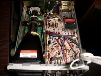
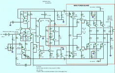
Getting closer (attachment 1) . Done the hard way. REAL hard. The power board will look pretty , I guess that is important , but it should be pretty free of parasitics and possible feedback (no outputs near inputs ,feedback loop wrapped with a ground trace).
This board will do either a Self EF2 or a EF3 (CCS or resistor) , use 3 pair OP's,large "hardware variety" fuses (5 x 30mm) , 6800uf onboard decoupling.
The voltage board will mate with European connectors / edge pin strips.
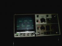
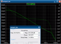
Scoped the Existing "supersym" with new scope (attachment 2/3) looks a little overcompensated at 20khz /80V with it big 68pF millers (rounded edges). For $20 , I could not resist a 20mhz hitachi scope (thats whats inside) ... no probes though. Time to make the Voltage board. When both are done I will submit them.
OS
This board will do either a Self EF2 or a EF3 (CCS or resistor) , use 3 pair OP's,large "hardware variety" fuses (5 x 30mm) , 6800uf onboard decoupling.
The voltage board will mate with European connectors / edge pin strips.
Scoped the Existing "supersym" with new scope (attachment 2/3) looks a little overcompensated at 20khz /80V with it big 68pF millers (rounded edges). For $20 , I could not resist a 20mhz hitachi scope (thats whats inside) ... no probes though. Time to make the Voltage board. When both are done I will submit them.
OS
Attachments
I've got a couple of suggestions but should clarify I've got no idea about PCB design/layout etc
Move the bias pot in a little so the track does not need to go under the two resistors. Add a pad to the pot so both inline and offset types can be used.
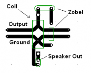
Fill in the track next to the Zobel (green tracks next to each other).
I've attached a free hand attemp to show what I mean
Cheers
Rob
Move the bias pot in a little so the track does not need to go under the two resistors. Add a pad to the pot so both inline and offset types can be used.
Fill in the track next to the Zobel (green tracks next to each other).
I've attached a free hand attemp to show what I mean
Cheers
Rob
Attachments
I've got a couple of suggestions but should clarify I've got no idea about PCB design/layout etc
1.Move the bias pot in a little so the track does not need to go under the two resistors. Add a pad to the pot so both inline and offset types can be used.
2. Fill in the track next to the Zobel (green tracks next to each other).
I've attached a free hand attempt to show what I mean
Cheers
Rob
There are a lot of tweaks I will still do , so I am still learning ,too. 🙂
As far as your #1 , I could eliminate 1 jumper (one of those resistors is a jumper), the bias pot is a good idea , since inline ones seem to be more common (mouser has both).
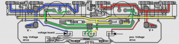
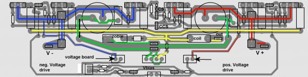
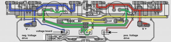
#2 ... my "take" on this is that the zoble return is a separate "garbage path" , mostly RF , that should be separate from the Rail returns. The rail returns should be equal length and width (symmetric). The 2 little green traces are for the small voltage board's decoupler's and the input ground (again separate) , all terminating at the main star.
I still have to give the output coil more room (10 X 20 MM) and general cleanup.
OS
couple more bits of filling in
No , No , NO !!!!
You fill them in , and you degrade performance. The output should be taken as close to halfway between the negative and positive "sides" as possible. As should the feedback and zoble. Treat the Output as you would the ground.
OS
sorry had already posted before you made the comments about ground etc, do you want the post deleted to stop confusion?
sorry had already posted before you made the comments about ground etc, do you want the post deleted to stop confusion?
No bother , hopefully I set you right. 🙂 This is "layout 101 " 🙄
OS
Also, maybe you could even out the space between output transistors some so that Sanken MT200 (like 2Sc2922) package devices can be used.
- keantoken
- keantoken
Hey Ostripper, your output coil is directly parallel to only one of the emitter traces! Oh the humanity!
I'm no expert myself but I am a perfectionist. How do you like this?
- keantoken
I do like that ,BUT , there are real world constraints ... ie- board space, physical component sizes ,etc. I am going to give the OP coil more space.
OS
or locate the R//L away from the PCB and away from the chassis panels.
Do you mean a separate board with both the zobel and L/C?
OS
no,
just the R//L off the PCB.
The R+C is an HF load for the amplifier and as such should have a defined HF impedance. Long leads and/or traces will introduce undefined inductance and potentially ruin the desired HF loading that the Zobel is intended to provide.
just the R//L off the PCB.
The R+C is an HF load for the amplifier and as such should have a defined HF impedance. Long leads and/or traces will introduce undefined inductance and potentially ruin the desired HF loading that the Zobel is intended to provide.
so happy ... 🙂🙂🙂🙂 my caveman paint shop pro technique does beautiful on an HP printer for PCB's (no anti-aliasing). It is so nice to have all your own equipment.
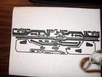
The Zipfile attached has all the schemas , artwork , parts placement for absolutely stunning toner transfers. (Attachment 1) I need to buy more toner , almost out. 😡
A couple of days from now the Voltage board will be done making for some sweet construction. 😎
The power board will look cool ,too . 2 red LED's , very good layout ... looks as well as low parasitics(attachment 2). One will have the option of all 3 varieties of EF's with 2 small jumpers on Q16 and 17. Also.. I was thinking of a trimmer for the main CCS of the amp. On the real one while scoped I could get the LTP much more symmetrical improving the sound further by adjusting the current slightly. This will also facilitate "fine tuning" for different power supplies.
The voltage board artwork and a verbose BOM with instructions on how to implement all the options (FET's , OPS , supply changes)will be done in a couple days. 🙂
OS
Attachments
discussion on C3 cascode transistor in VAS
Hi Ostripper
I have been following his agreements Symasym ... and Mongrel.
In his Supersym T3T amplifier, you eliminated Q6 the cascode transistor , to be able to use C7 the Miller compensation, and replaced it with the employment of a R48 // C6.
In his Mongrel amplifier you support Q11 the cascode transistor and place C3 the miller capacitor.
I´m interested in to know which is the function of the cascode transistor . Since in the original Otalla – Hitachi design the cascode transistor is not. Or which are his reasons not to use the configuration of the T3T in the Mongrel amplifier.
Attachments
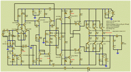
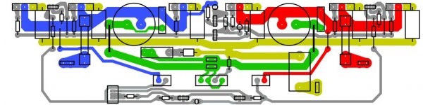
All done with the boards , A new (and hopefully) final schema (below).
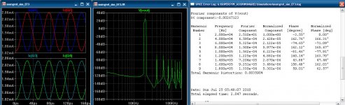
Now I have to order all the little parts. So ... a BOM is coming , very detailed ,with mouser part #'s. I had to finalize all the MODS that the board can do (EF2 , EF3 , and J112 FET's). The simulations are all in attached " mongrel_sim_all.zip".
I did all these modifications on the real "supersym" WITH my new scope , so all is good to go ...(no )
)
What you see on the plots was confirmed in the real world , so to hell with those who say simulations are "lies". EVERYTHING in the simulation coincided with what readings I collected in the "real world" .. currents , waveforms all within a few % 🙂 .
The colored PCB overlays which I show below are my form of "visualization" to get the PCB artwork right for symmetry and grounding. BTW , the red outline on the schematic is what is on the power board.
My thanks to the Bob Cordell power supply interview , Nelson Pass's discussion on cascodes ,and ESP audio's project 15 (capacitance multiplier) that I added to the power board.
This project is different, as one can swap Voltage stages and run a DX style amp , Self amp , ... anything. Don't have to tear up the project to try something new , A TRUE DIY class AB project.
Edit , I have to post again to get the artwork on (very large 1200dpi )
OS
Now I have to order all the little parts. So ... a BOM is coming , very detailed ,with mouser part #'s. I had to finalize all the MODS that the board can do (EF2 , EF3 , and J112 FET's). The simulations are all in attached " mongrel_sim_all.zip".
I did all these modifications on the real "supersym" WITH my new scope , so all is good to go ...(no
)What you see on the plots was confirmed in the real world , so to hell with those who say simulations are "lies". EVERYTHING in the simulation coincided with what readings I collected in the "real world" .. currents , waveforms all within a few % 🙂 .
The colored PCB overlays which I show below are my form of "visualization" to get the PCB artwork right for symmetry and grounding. BTW , the red outline on the schematic is what is on the power board.
My thanks to the Bob Cordell power supply interview , Nelson Pass's discussion on cascodes ,and ESP audio's project 15 (capacitance multiplier) that I added to the power board.
This project is different, as one can swap Voltage stages and run a DX style amp , Self amp , ... anything. Don't have to tear up the project to try something new , A TRUE DIY class AB project.
Edit , I have to post again to get the artwork on (very large 1200dpi )
OS
Attachments

Last edited:
- Home
- Amplifiers
- Solid State
- The MONGREL (supersym II)