The Cdom at the grounded base cascode should be increased to 220p. If you suspect simulation isn't showing us all the details, then the next logical step is to build it and find out. At least if it fails we'll know in the future what not to do, instead of being afraid to do it and regretting that we did not.
- keantoken
- keantoken
The Cdom at the grounded base cascode should be increased to 220p. If you suspect simulation isn't showing us all the details, then the next logical step is to build it and find out. At least if it fails we'll know in the future what not to do, instead of being afraid to do it and regretting that we did not.
- keantoken
Keen , I made a discovery. we have been going after low distortion while forgetting about THE SOUND. Below (attachment) , I went back to the "baseline" design , the original symasym. I was always afraid of the shunt compensation in the original. by putting that fear aside , I used the symasym shunt comp. and just 1 cdom like the original. It was pleasing to see the 2nd dominant at all power levels with the 3rd , 5th , 7th stepping down after. 🙂
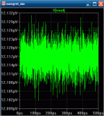
I did not see this before YOU gave me that -150db noise floor .. THANX.
BTW , The distortion was a little reduced (not as much as yours) , but the harmonics are a dead match for the original "sym".
This is my major design goal , the sound.. we have a symasym with 4 times the power ,1/10 the distortion ,tighter OPS/Vbias ,and superior PSRR.
edit - I must see what this does to the bode plot. A little more fiddlin' .
OS
Attachments

Last edited:
Are you sure ? what are R15-17?(attachment 1 - A) ...
OS,
I can't see what do you have in your computer. Your schematic from post #1 does not contain the R15-15 resistors. 🙄

Very close to final 😀 schematic and BOM. Guaranteed to work (already have 2) , will sound at least as good as symasym but with much more headroom.
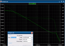
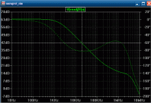
EDIT : final OLG plot ... unity gain 970khz (below )
OS
EDIT : final OLG plot ... unity gain 970khz (below )
OS
Attachments
Last edited:
Looks good to me. Preserving the original behavior is a noble goal. After all, Symasym has been proven to sound good...
- keantoken
- keantoken
Looks good to me. Preserving the original behavior is a noble goal. After all, Symasym has been proven to sound good...
- keantoken
Thanks , your simulation help was invaluble , SIR ! 🙂
Now you can watch a fool and his amp at work... yeeh haw! This is the part I like.
First , the patient ... [attachment 1] 100lbs of BURNING AMP !!
 just kidding...
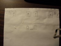
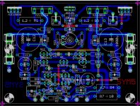
Second , measure the heatsink OPS mounting holes with paper , I will use 3/4 's
of available heatsink space for a very low c/watt , a 12" X 3" FR-4 will do for the current stage.
Third , start to draw ... love it...
BTW , there are your amps .. all hand drawn (august maybe , I will keep a promise) gave the frugalamp 3 to "danielwritesback" (member)
First pix with my new 12m pixel camera ...
We can still work on the voltage stage , I will leave the mini board (2X3") very "open ended" to accommodate various compensation "tweaks" . with separate
boards the possibilities are endless. I will also REALLY refine the grounding and be VERY vigilant about parasitics in the layout stage.
OS
Attachments
Last edited:
Will the layout be similar to Symasym? I seem to remember Mike making some comments about changing the layout and getting worse performance. It seemed the current layout is optimal.
- keantoken
- keantoken
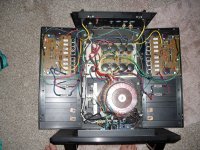
Yes , layout is as hard as the design/simulation phase.
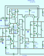
If you look at the board below , there is no real issue. The ground and rail traces , at least in my opinion should be totally symmetrical (mine are , like a butterfly).
He kept the input and OP physically separated as well as the ground taps for in vs. out. (green lines are ground , blue is rails)
The reason for total symmetry (trace length , thickness) is that the pulses from the rail decouplers should meet right at the middle. Same with the OPS emitter resistor traces .. absolutely mirror image to create a perfect center point for the NFB takeoff.
The symasym is a much lower current creature than a supersym or mongrel , so this is not as critical. The mongrel won't even have the sensitive voltage amp on the same board with all that dirty current .. so that is solved. The Current stage will be total butterfly (mirror image) with a true 360 "star" because we are dealing with 6-8 amps at times. In short , the bigger amp HAS
to be laid out better to assure good performance.
OS
Attachments
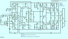
Keentoken was on the right track , on this type of VAS one must use a pole-zero cancellation frequency compensation technique. It uses one pair of complex zeros to cancel one pair of complex poles, resulting in feature that the frequency response of the amplifier exhibits that of a single-pole system.
For this to work , at least with a THIS balanced VAS , one must either do some math 😡 or experiment with different ratio's of the two miller caps. Thanks to one of Dr. Bora's excellent designs , I know the ratio (8/1 - C3/ C4). Wrapping the large miller (220pF) around the VAS cascode allowed me to use a 27pF for the VAS output side. This made the simulation "sing" .... Distortion dropped 6-10db and was faster to beat. Just a little change in compensation (C17) corrected my phase margin. On top of this I gained better slew and square-wave response by a large margin. Strange , but OLG increased by 8DB allowing for me to "burn-up" more with the load resistors.
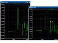
On the symasym , the R/C load at the VAS output does 2 things , it linearizes the VAS slightly and acts as the 2nd dominant pole for the vas. On my faster devices , I only needed the resistive load to accomplish the GOAL (sound quality , correct harmonic residual). With a 100k symmetric load across the collectors of the VAS , I can "trade" H2 for H3(attachment 2). Different values can be used to determine the amps harmonic character, thus it's final sound.
As far as SPEC's.. wow. THD20 = .001% 40V p-p .003% 90V p-p. The only way I can exceed .01% is to simulate a 20KHZ - 2R load at almost 120V P-P !
I will simulate with my T3T triple just for laughs and giggles but I still want to keep it simple (EF 2/3).
(attachment 1 is MINOR change in circuit)
OS 🙂🙂🙂
For this to work , at least with a THIS balanced VAS , one must either do some math 😡 or experiment with different ratio's of the two miller caps. Thanks to one of Dr. Bora's excellent designs , I know the ratio (8/1 - C3/ C4). Wrapping the large miller (220pF) around the VAS cascode allowed me to use a 27pF for the VAS output side. This made the simulation "sing" .... Distortion dropped 6-10db and was faster to beat. Just a little change in compensation (C17) corrected my phase margin. On top of this I gained better slew and square-wave response by a large margin. Strange , but OLG increased by 8DB allowing for me to "burn-up" more with the load resistors.
On the symasym , the R/C load at the VAS output does 2 things , it linearizes the VAS slightly and acts as the 2nd dominant pole for the vas. On my faster devices , I only needed the resistive load to accomplish the GOAL (sound quality , correct harmonic residual). With a 100k symmetric load across the collectors of the VAS , I can "trade" H2 for H3(attachment 2). Different values can be used to determine the amps harmonic character, thus it's final sound.
As far as SPEC's.. wow. THD20 = .001% 40V p-p .003% 90V p-p. The only way I can exceed .01% is to simulate a 20KHZ - 2R load at almost 120V P-P !
I will simulate with my T3T triple just for laughs and giggles but I still want to keep it simple (EF 2/3).
(attachment 1 is MINOR change in circuit)
OS 🙂🙂🙂
Attachments
How about PSRR? Output impedance? Or I can generate plots if you'll hand me the latest simulation.
Does R10 need to be plugged in to signal ground? I would minimize unnecessary currents through the 10R resistor, and this connection might inject a little rail noise across the resistor.
Is R11 necessary? Q8 will be more linear with higher Vce.
If I were you (but I'm not), I would replace the input and feedback voltage sources with capacitors again, simulate, tune offset if necessary, measure offset across the caps and replace them with voltage sources of these values. The current values are "old" (unless you updated them) and are probably introducing a little offset.
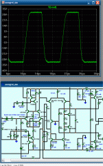
Also, this amp will reproduce square waves flawlessly with C2 so large, as it will absorb any difficult signals. For truly inspecting square response behavior my preference is to make C2=C17, I find this a fair way to treat the amp for testing.
Sorry for hijacking your thread earlier.
It's getting more final all the time.
- keantoken
Does R10 need to be plugged in to signal ground? I would minimize unnecessary currents through the 10R resistor, and this connection might inject a little rail noise across the resistor.
Is R11 necessary? Q8 will be more linear with higher Vce.
If I were you (but I'm not), I would replace the input and feedback voltage sources with capacitors again, simulate, tune offset if necessary, measure offset across the caps and replace them with voltage sources of these values. The current values are "old" (unless you updated them) and are probably introducing a little offset.
Also, this amp will reproduce square waves flawlessly with C2 so large, as it will absorb any difficult signals. For truly inspecting square response behavior my preference is to make C2=C17, I find this a fair way to treat the amp for testing.
Sorry for hijacking your thread earlier.
It's getting more final all the time.
- keantoken
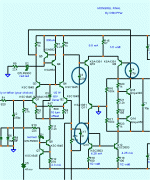
Alternative compensation hook-up
Hi Ostripper, did you consider returning the compensation caps to the emitters of Q3/Q4?
Those emitters provide a low impedance point and make the compensation path "unidirectional". Also the emitter voltages refer to ground, rather then the 1kOhm pull-ups referring to V+ rail, improving high frequency PSRR. [The output stage input node (the other end of comp cap C4) refers to signal ground, so the comp cap will inject supply trash straight into the output. When returning C4 to the emitter of Q3, it will be ground referred on both sides, redering it harmless for PSRR. For C3 you could halve the injection, as the other end is V- rail refered.]
That is a good idea , in simulation it works as well as the present comp. , a small change to make for psrr improvements.
Below is schema as it is now , another with alt. compensation (is that right , Jeepee) and the latest .asc file.
OS
Attachments
by keentoken - If I were you (but I'm not), I would replace the input and feedback voltage sources with capacitors again, simulate, tune offset if necessary, measure offset across the caps and replace them with voltage sources of these values. The current values are "old" (unless you updated them) and are probably introducing a little offset.
WAY tuned (below) wanted to see what noise this amp put out with different devices. 😎
OS
Attachments
By ostripper - That is a good idea , in simulation it works as well as the present comp. , a small change to make for psrr improvements.
What I found is that Jeepee's change extends OLG way into the MHZ , while stable , I would have to either drastically increase miller capacitance (330/56pF) or degenerate the LTP (100R+) to get back to the "target" (800k-1mhz UG).
OS
Attachments
Hi Ostripper,
That's indeed what I had in mind.
BTW: what's the purpose of C3? It's connected to a low impedance point (the input impedance of the current mirror) so it's hardly effective as Miller compensation. Isn't it merely loading Q10? Due to Q11, Q10's Miller effect must be small anyway. What happens without C3?
another with alt. compensation (is that right , Jeepee)
That's indeed what I had in mind.
BTW: what's the purpose of C3? It's connected to a low impedance point (the input impedance of the current mirror) so it's hardly effective as Miller compensation. Isn't it merely loading Q10? Due to Q11, Q10's Miller effect must be small anyway. What happens without C3?
By Jeepee- what's the purpose of C3?
Without it the simulator "chokes" dead... no OP.
 will work good with typical 47-68p miller for C4 , but with more distortion.
Also ,the real amp has a 68p for both C3-4 (typical / ampslab ,otala,hitachi) , and it has worked for a year.
OS
Last edited:
I see.
Thinking aloud here...
There are 2 path to the output stage:
path 1 = Q3, R5, Q9
path 2 = Q4, R6, Q10.
On path1 the conventional Miller compensation (C4) is applied. C4 renders Q9 into a transimpedance stage, with a increasingly more effective voltage output behaviour at high frequencies, driving the voltage input of the output stage. A tried and tested technique. Path 2 provides double the gain, when summed via current mirror Q13/Q12. Q12 output is a current source, also for high frequencies. The compensation cap C3 renders Q10 into a voltage source. However this voltage source will not be very effective, looking into the emitter of cascode Q11 (killing local loopgain and loading the transimpedance stage with a low impedance). So I can only arrive at the conclusion that C3 merely works as a filter. In that case C3 is just as effective directly accross the Q13/Q12 mirror node to the V- rail (also better for PSRR).
Maybe increasing C3 in that new position helps. At low frequency you start of with a fully balanced system with twice the loopgain, then for progressively higher frequencies the loopgain is lowered by C3 filtering, killing the mirror path for high frequency. That way you arrive back at the "conventional" design with 1 Miller compensated VAS at the critical stability area.
What do you think, worth a try?
By Jeepee - In that case C3 is just as effective directly accross the Q13/Q12 mirror node to the V- rail (also better for PSRR).
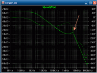
Tried that .. below is what I got (att. 1) ,and why (att. 2).
see peak .... (arrow)
OS
BTW , amp is doing 50+v /uS symmetrical slew at 20k , another design goal.
Attachments
Last edited:
A well-placed resistor might dampen that peak, but I haven't found out where yet.
I don't think the simulator can take us much farther, I think it is time to build.
Also, what is the risetime for your square source? Most amps can take several uS with ease. Try decreasing to several nS or lower.
- keantoken
I don't think the simulator can take us much farther, I think it is time to build.
Also, what is the risetime for your square source? Most amps can take several uS with ease. Try decreasing to several nS or lower.
- keantoken
- Home
- Amplifiers
- Solid State
- The MONGREL (supersym II)