Hi Tinitus,
Regarding layout,
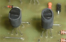
The idea is to have the flat portion of the TO-92 pairs facing each over (just as in ostripper's layout), making thermal coupling possible. Diffential and current mirror pairs respectively benefit from thermal coupling.
Ostripper, I follow your design development with great interest, great work!
Regarding layout,
The idea is to have the flat portion of the TO-92 pairs facing each over (just as in ostripper's layout), making thermal coupling possible. Diffential and current mirror pairs respectively benefit from thermal coupling.
Ostripper, I follow your design development with great interest, great work!
Hi Tinitus,
The idea is to have the flat portion of the TO-92 pairs facing each over (just as in ostripper's layout), making thermal coupling possible.
it easy enough to make your own "heatsink-coupling"
and it doesnt matter how they turn, as long as they are in line
works either way, no problem, if thats the priority
Hi OS,
But the current trough Vbe is not constant for CX.
dado
The current through VAS is defined by LTP constant current source. OS has chosen (deliberately or not) to use a current source with negative temperature coefficient dI/dT<0, while VAS has positive temperature coefficient dI/dT>0, so he got pretty stable VAS current regarding temperature change. 🙂
it easy enough to make your own "heatsink-coupling"
and it doesnt matter how they turn, as long as they are in line
works either way, no problem, if thats the priority
Hi tinitus,
Sorry if you took my response as crititism, i did not mean to do so but I realised afterwards that I should have put it differently.
No it does not work as well I'm afraid. There is a distance and distance will introduce a delay transfering heat. Maybe minor details but I think it's easier tying two close transitors than two far apart.
Further, in a mirror pair you don't want wide track from any transistor to a heat generating component such as a resistor. A wide trace transfer more heat to one of the transistors. And of course close tracks will be closer in temperature than traces placed far apart.
Bluesky, because of the current mirror the tempco of the LTP CCS won't be important, no? Unless the current mirror is saturating, because the joined collectors will ignore the VAS' Vbe. Furthermore, how much will Ib tempco matter considering the tempco/imbalance effects introduced by small differences in CM Vbe's?
BTW, I'm running Linux too, though I can hardly figure it out.
- keantoken
BTW, I'm running Linux too, though I can hardly figure it out.
- keantoken
Hi tinitus,
Sorry if you took my response as crititism..........
hey, thats what we are here fore, nothing gets anywhere without it 😉
but I think you are wrong in what you say about direct couling
sure, they will have quicker reaction on each other
but is that what you really want
if coupled to a certain mass of alu or copper, they will have equal temperature always
differences will be very limited
well, I can say that, noone knows for sure anyway, and enough of it 😀
and like it or not, its really none of my concerns, its not mine, its ossies baby, he will know what matters to him 😉
I just get this funny urge whenever I see a layout, and I can only recommend to try , its good practice and learning 🙂
I think you have this wrong.if coupled to a certain mass of alu or copper, they will have equal temperature always
Im not surpriced you say that 😀
a very bold claim, yes
I know if I suggested common practice, to glue them together, I would be right 🙄
point is, I really dont know, either way
a very bold claim, yes
I know if I suggested common practice, to glue them together, I would be right 🙄
point is, I really dont know, either way
The current through VAS is defined by LTP constant current source. OS has chosen (deliberately or not) to use a current source with negative temperature coefficient dI/dT<0, while VAS has positive temperature coefficient dI/dT>0, so he got pretty stable VAS current regarding temperature change. 🙂
yes, just about everything I do is deliberate. Actual testing in the real world between 0c and 40c shows just uA changes in the VAS. 🙂
Tinitus , the input pairs are deliberate ,too. I tried to eliminate as many jumpers as possible without having to use microtraces between devices while maintaining "face to face" contact. Not using "face to face" would be acceptable , but not as refined as doing so. The real amps can maintain .1mv offset , even outdoors (windy , wild temp. swings) I test for this as some of these amps are being used in a mobile environment.
By tinitus ,Im not surpriced you say that
a very bold claim, yes
I know if I suggested common practice, to glue them together, I would be right
point is, I really dont know, either way
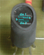
I have broken open to-92 devices with the hammer after "screwups" (I do these too 🙁 ) , the die faces the flat side and is much closer to it as well. The thermoplastic on the curved side is 5 times thicker and not the best thermal conductor. wrapping a pair with a thin strip of copper might solve this , but "face to face" with a closely matched pair heat-shrinked together is best (below).
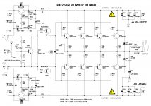
Wait till you see my new powerboards. (2 BJT's -1 L mosfet / split ground and split rails) 😉
OS
Attachments
so it does have a significant effect
well, I admittedly thought of it as mostly a "fashion"
ok, thanks
btw, occatinally I work with Araldite epoxy
it would be easy to "build" a ball of epoxy around them
while its hardening and still soft, it would be easy to cut it into a nice shape
well, I admittedly thought of it as mostly a "fashion"
ok, thanks
btw, occatinally I work with Araldite epoxy
it would be easy to "build" a ball of epoxy around them
while its hardening and still soft, it would be easy to cut it into a nice shape
The small signal differential devices in a high loop gain power amp are EXTREMELY sensitive to the environment. One can hold a lighter or other heatsource 100mm distance from the flat side and the device(the die) "sees" the infrared ...corresponding to a .2mv - .5mv amplifier offset change even without any direct contact 😱. A monolithic pair has the 2 devices on the same die , which is even more ideal. For the poor man , at $.10c apiece, .. face to face is very cost effective. I do not tolerate the 10-50mv offsets that are acceptable to other enthusiasts , <2mv is what I usually get before I tweak my "CCS adj. and "Offset" trimmers (.2-.5mV - all done 🙂 ). BTW , "face to face" , you can heat the whole pair with a lighter and offset will not change much , if any.
I should of used the pix above to illustrate , (below is better).
OS
I should of used the pix above to illustrate , (below is better).
OS
Attachments
Last edited:
One can hold a lighter or other heatsource 100mm distance from the flat side and the device(the die) "sees" the infrared ...
well, that is exstreme
Wait till you see my new powerboards. (2 BJT's -1 L mosfet / split ground and split rails) 😉
OS
You're killing me!😀
OS is the new DX...😀
Nice work friend! CX, PX, AX, where's the SEX?

What are you using for layout these days Pete? Looks real good.
Nice work friend! CX, PX, AX, where's the SEX?
What are you using for layout these days Pete? Looks real good.
You're killing me!😀
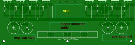
(Below-1) is what will fit a 100mm (@4") conrad heatsink. Anything beyond 87mm (3.5") will work. The voltage board will stand up at 90 degrees from the "_X - voltage board" pins , screwed down with standard 2-position euroblocks.
The present PB250 (8 device) was designed custom for my Genesis chassis ... this one only takes up a 80 x 80 x225mm footprint.
The lateral MOSFET .."goldmund killer" will be similar to this as well with the ability to use any voltage board. (PB250BJT/LFET)
2 half- sized 4 device boards are coming , too (PB120BJT/LFET)
OS is the new DX...
Nice work friend! CX, PX, AX, where's the SEX?
What are you using for layout these days Pete? Looks real good.
I am using Sprint layout and S-plan (German made).The "macros" (actual parts) are custom made by me (sprints libraries are dated). I want this to be the new Class-AB standard. You can just sim/design/etch/plug-in without reworking the whole thing. I already have tried 6 different topologies (a-g X).. all work good !
I am porting all of it to the sprint software so enthusiasts can have pro boards made (gerbers , excellon , drill data) ... all this is included in the finished ZIP's (.LAY) or separately if they ask.
SEX is a good name for one of them , if any are real "good in bedding down"(ahh ,capacitors that is) , I'll think on that. 🙄 If you notice , I have no module called "DX" .. that is patented..

OS
Attachments
Last edited:
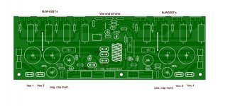
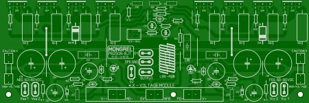
PB250N almost there,very purrdy board.
Wheww! My first big board on sprint is almost done. Decided to just put the multipliers on board like my proven main home amp (the PB250 in the genesis case). It is an exact copy of my amp , but different caps and layout. If enthusiasts want to go crazy with regulated supply , I will make a separate board.
To avoid what was a "trainwreck" on the goldmund ripoff amp (60VAC right on board 🙁 ) , a separate unregulated supply would need to be built anyway !!! Why not combine the unregulated PS WITH the shunt regulator and run JUST clean DC ( +/ - 80V) , to this nice clean board ??
G1 and G2 split grounds will mate well with the massive PS100 capacitor board.
"Just about finished" product below (tomorrow-done). NFB takeoff/main coil are centered , Rails are even balanced ... the Vee/Vcc2's can be jumpered for single power supply's as well. It sure helps to have the prototype (my amp) to go back to. 🙂
OS
Attachments
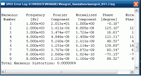
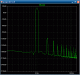
Os another goldmund killer version you should look at if you like Jfets is to use cfp. Using Jfets you need them to be cascoded and when used in bjt cfp you take care of memory distortion and ultra stable LTP. As the LTP gm has a hefty increase and the jfet is linearized because of the local feedback, distortion drops buckets, I think it will outperform your version if you use high gm jfets like 2sk170 or bf862 especially at high frequencies, 20khz. Another big plus is that the Jfet bjt cfp combined with cascode sound very good, to me the best LTP combination for my ears. It has practically no effect on the harmonic spectrum. On one of my car based amps using this topology I managed a measured .004THD at 20khz 150 W before clipping using 2sk363 as the Jfets. On the vas LTP no buffering is required and a little mod to the current mirror will get you symmetrical slew.
Os another goldmund killer version you should look at if you like Jfets is to use cfp. Using Jfets you need them to be cascoded and when used in bjt cfp you take care of memory distortion and ultra stable LTP. As the LTP gm has a hefty increase and the jfet is linearized because of the local feedback, distortion drops buckets, I think it will outperform your version if you use high gm jfets like 2sk170 or bf862 especially at high frequencies, 20khz. Another big plus is that the Jfet bjt cfp combined with cascode sound very good, to me the best LTP combination for my ears. It has practically no effect on the harmonic spectrum. On one of my car based amps using this topology I managed a measured .004THD at 20khz 150 W before clipping using 2sk363 as the Jfets. On the vas LTP no buffering is required and a little mod to the current mirror will get you symmetrical slew.
That is a cool idea .. I did play with BJT CFP LTP's a while ago. With my mongrel lineup , making a modded voltage board would be easy as cake. 🙂
A lot easier than my new PB250. This took me 4 hours schema/Bom/PCB ... 1 hour from this post , it will be in "PB250N_BJT.ZIP" on my website. I am at the point of export from the fine German software (sehr gut!! ) 😀
The BOM will be simple , with many options for sourcing. the PB120N is almost there as well. NO "RABBITHOLE" simulations to PCB here.. this is my main home amp !!! So it freakin' works (3+ months now) ... beyond prototype. 🙂
Examples below...
OS
Attachments
Big board. Many outputs.
I like the modular approach - nice work OS 🙂
Thanks MJL , I owe it to you for the "lust for pretty boards" back in your old threads. I have the toner transfer perfected .. NO pits/undercut and with the sprint .. better layouts. With modular prototyping is a breeze , the PB's interface has the voltage board upright , saving considerable space. The PB120 I will make next will definitly fit in a 5.1 case but still be modular. 🙂
Ahh , "many outputs" will get your heart beating with 1/2 KW transients. You think .. why don't they sell this stuff in walmart??
You came so close with your abomination a year ago.. wanna know how far it can go ?? look below - no lie. The perfect amp ???
 Scaled down with 20V rails would make for the perfect headphone amp.
OS
Attachments
Last edited:
- Home
- Amplifiers
- Solid State
- The MONGREL (supersym II)