Hi,
the Leach is biased by the Optimal ClassAB method.
The device bias is determined by the Re value and the Vre across that emitter resistor.
The Total output bias for Xpairs of output devices is Vre/Re * X
Using Leach's Re=0.33 and Vre= 20mV. Then a 2pair Lo Tim has a total bias of 0.020/0.33 * 2 = 120mA.
I one keeps the same Re value and chooses to use 3pair then the total bias turns out to be ~180mA.
Going back to the standard 2pair Leach with a voltage amplifier stage, Pre-drivers and Drivers, the total quiescent current is ~150mA
thanks for the reminder......
andrewt,
prof leach use 470/680r on protection emitter resistor (sensor),
jens use 330r on his 5 pair,
if i make 10 pair what will be the value of the sesor,.
regards.
prof leach use 470/680r on protection emitter resistor (sensor),
jens use 330r on his 5 pair,
if i make 10 pair what will be the value of the sesor,.
regards.
the value of the protection components varies with:
the output device SOAR,
the output device temperature,
the PSU voltage,
the charge held in the smoothing caps,
the emitter resistor in the output stage,
the transient capability of the output stage,
the transformer regulation,
the size of the heatsink,
the value of bias current.
I cannot give a simple answer. I am not prepared to investigate every different combination of all these variables.
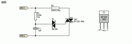
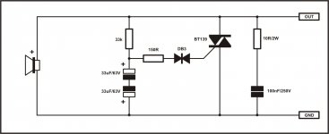
the circuit shown above have not the same use at all: it is speaker protection against DC burst in the signal, it is not ouput transistor protection
A BR100 is about 30V, way too high for DC fault protection.
Use a 2N4991, about 8V.
2N4991 pdf, 2N4991 description, 2N4991 datasheets, 2N4991 view ::: ALLDATASHEET :::
Use a 2N4991, about 8V.
2N4991 pdf, 2N4991 description, 2N4991 datasheets, 2N4991 view ::: ALLDATASHEET :::
I suggest you do a little experimenting with the bias setting if the amp is finished and you can input music. As I tweaked the bias pot I could hear a major improvement in the bass response and overall tonal quality of the music. At a very low setting the music was just dead. This amp layout was never intended to be a class A amplifier I just upped the bias to a point that sounded very good to my ears. When and if in doubt go to the Leach amp website and construct the amp as Dr. Leach recommends. That would be the proper method from the individual who designed the layout.
Bob Ellis and some others have done a very good job on explaining the protection circuit and providing insight into what particular resistor values are needed for all of the available voltage combinations. If I get some time I will try and find the files and post them here.
Tad
Bob Ellis and some others have done a very good job on explaining the protection circuit and providing insight into what particular resistor values are needed for all of the available voltage combinations. If I get some time I will try and find the files and post them here.
Tad
With my "correction" here
http://www.diyaudio.com/forums/grou...mp-pcb-group-buy-interest-64.html#post2364365
Brian
http://www.diyaudio.com/forums/grou...mp-pcb-group-buy-interest-64.html#post2364365
Brian
Pingrs,
I in no way wished to exclude you from the excellent work you contributed I just did not have all of the information in front of me this morning and relied on a stored document file. Many thanks for your contribution and helping to unravel the protection circuit debacle.
Tad
I in no way wished to exclude you from the excellent work you contributed I just did not have all of the information in front of me this morning and relied on a stored document file. Many thanks for your contribution and helping to unravel the protection circuit debacle.
Tad
Is this for PA or hi-fi?
If hi-fi use class G,
http://www.crestaudio.com/media/schematics/8001_schematic_set1.pdf
for PA class H may be acceptable (may not be for HF).
http://www.crestaudio.com/media/schematics/8002_schematic_set1.pdf
If hi-fi use class G,
http://www.crestaudio.com/media/schematics/8001_schematic_set1.pdf
for PA class H may be acceptable (may not be for HF).
http://www.crestaudio.com/media/schematics/8002_schematic_set1.pdf
@asia, are you going to build one yourself?
i got quotes for Kanwar's 1.5kw classH amp, have you seen it? http://www.diyaudio.com/forums/solid-state/180638-diy-1-5kw-bipolar-class-h-3.html#post2438741
i got quotes for Kanwar's 1.5kw classH amp, have you seen it? http://www.diyaudio.com/forums/solid-state/180638-diy-1-5kw-bipolar-class-h-3.html#post2438741
Last edited:
Hi,
a two pair Leach driving ~150W into 8r0 performs well.
The voltage requirements and the current demands match up well.
Change to a 3pair and the Leach can drive a slightly lower impedance.
If one wants a Leach to drive low impedances to high voltages then current demand becomes the critical concern. A 3pair Leach cannot effectively pass the current demanded by a reactive 2ohm speaker.
You can fiddle with SOA using multiple supply rails for short term voltage requirement, but that does not solve the problem of meeting the current demands of the low impedance load.
Take a comparison.
150W into 8r0 requires 49Vpk and 6.1Apk at the resistive load.
For reactive speaker loading allow for transient peak current demand <=18.3Apk
Now compare the current demand of the same amplifier driving a reactive 2ohm load.
This will try to give 600W into 2r0 and require 49Vpk and 24.5Apk into the resistive load.
The 2ohm reactive speaker load can demand upto 73.5Apk. A 3pair output stage would require each output device to pass ~24Apk on fast transients to the load. What is the transistor gain when passing 24Apk?
How much current does the driver need to supply to allow the outputs to pass that transient current peak?
A 6pr or 10pr output stage stands a chance of meeting the current demands of a low impedance reactive speaker. ClassX, Y, or Z only help with SOA and voltage requirement. They do not address peak current demand.
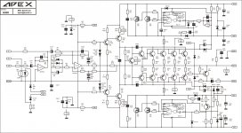
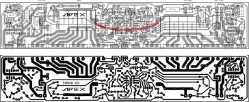
how about apex h900 step + leach?
if you want to classH a leach amp, then you will need to change all trannies that can withdtand rails of +/-95volts....
to give 600W into 2r0 and require 49Vpk and 24.5Apk into the resistive load.
The 2ohm reactive speaker load can demand upto 73.5Apk. A 3pair output stage would require each output device to pass ~24Apk on fast transients to the load.
A graphical illustration might be of help to Noob like me, i "use to think" reactive loads also demands "finite amount of current at zero crossings" [due to current being not in phase with voltage] thereby causing a condition to built up which is having both high VCE and IC at the same time across the device and increasing device dissipation very high.
- Home
- Amplifiers
- Solid State
- The Leach Amp