Not at all - It's incredibly simple;
V+ (pin 3)
V- (pin 1)
In (pin 2)
Out (pin 4)
A single-sided board will be fine, that's why there are starwashers on both sides as shown here
V+ (pin 3)
V- (pin 1)
In (pin 2)
Out (pin 4)
A single-sided board will be fine, that's why there are starwashers on both sides as shown here
Some very timid members have sent me private messages along the lines
When I reply "ask the entire community" it doesn't seem to happen.
One way to answer the question is to tabulate the individual tasks. First comes PCB footprints. As you will quickly learn, member 6L6 is very particular about footprints: he (rightly!) insists that you make the resulting boards easy to read, easy for newbies to solder, and easy for Lunatic FanBois to shoehorn in some crazy additional parts that aren't on Nelson Pass's schematic.
So plan on laying out each footprint once, and plan on revising each one at least once.
Looking at the very handy M2x Bill Of Materials, I count seventeen different footprints that you'll need to lay out: horizontal_mount_resistor, 3W_resistor, tiny_capacitor, input_module, ... etc.
Proceed in this fashion, going through all the other BOMs of the various daughter cards, counting up the number of different footprints they require.
Then estimate how long it will take you to create this number of footprints in your PCB CAD system. I predict your answer will be somewhere between 0.5 and 2.0 man-days. Or person-days if you prefer.
Now study the schematic of the amplifier board. Study the mechanical drawing of the diyAudio Universal PCB Mounting Specification. How long do you think it will take YOU to lay out this amplifier circuit, while remaining mechanically compatible with the Mounting Spec? That completely depends upon you and I have no way of guessing how slow or fast you are able to lay out PCBs. I'm sure it will take you at LEAST one full day and I would be shocked if it took you more than fifteen days. But these are so far apart that they aren't really too useful.
Then estimate how long it will take you to create the mirror image PCB. (Channel A and Channel B are different PCB layouts, in order to keep the input stage far away from the power transformer, and in order to keep the output transistors near the bottom edge of the heatsink (hot air rises!)). I imagine a good answer is: one third the amount of time it took to create the first PCB.
Then estimate how long it will take you to lay out each of the four daughter cards. Ponder "Norwood" carefully; since it's all-SMD, you may want to lay it out and fab it as a single layer board. This may take longer to lay out than a two layer board.
Then you'll need to have a few copies made, of each board type. I happen to like the Chinese fabs that appear when you get a price quote from PCBShopper – A Price Comparison Site for Printed Circuit Boards but please feel free to use whichever prototyping service YOU like.
How hard would it be to lay out the PCBs again, this time with "Frammiss Connectors" instead of bolts?
One way to answer the question is to tabulate the individual tasks. First comes PCB footprints. As you will quickly learn, member 6L6 is very particular about footprints: he (rightly!) insists that you make the resulting boards easy to read, easy for newbies to solder, and easy for Lunatic FanBois to shoehorn in some crazy additional parts that aren't on Nelson Pass's schematic.
So plan on laying out each footprint once, and plan on revising each one at least once.
Looking at the very handy M2x Bill Of Materials, I count seventeen different footprints that you'll need to lay out: horizontal_mount_resistor, 3W_resistor, tiny_capacitor, input_module, ... etc.
Proceed in this fashion, going through all the other BOMs of the various daughter cards, counting up the number of different footprints they require.
Then estimate how long it will take you to create this number of footprints in your PCB CAD system. I predict your answer will be somewhere between 0.5 and 2.0 man-days. Or person-days if you prefer.
Now study the schematic of the amplifier board. Study the mechanical drawing of the diyAudio Universal PCB Mounting Specification. How long do you think it will take YOU to lay out this amplifier circuit, while remaining mechanically compatible with the Mounting Spec? That completely depends upon you and I have no way of guessing how slow or fast you are able to lay out PCBs. I'm sure it will take you at LEAST one full day and I would be shocked if it took you more than fifteen days. But these are so far apart that they aren't really too useful.
Then estimate how long it will take you to create the mirror image PCB. (Channel A and Channel B are different PCB layouts, in order to keep the input stage far away from the power transformer, and in order to keep the output transistors near the bottom edge of the heatsink (hot air rises!)). I imagine a good answer is: one third the amount of time it took to create the first PCB.
Then estimate how long it will take you to lay out each of the four daughter cards. Ponder "Norwood" carefully; since it's all-SMD, you may want to lay it out and fab it as a single layer board. This may take longer to lay out than a two layer board.
Then you'll need to have a few copies made, of each board type. I happen to like the Chinese fabs that appear when you get a price quote from PCBShopper – A Price Comparison Site for Printed Circuit Boards but please feel free to use whichever prototyping service YOU like.
Here's what the daughter cards look like. Size is 40mm x 35mm, bolts are metric M3. Centers of bolt holes are inset 4mm from edge, except pin #3 which is intentionally asymmetric. This makes it very very difficult to install the card in a wrong orientation. (Nothing is impossible if you have a big enough hammer).
Leave some extra copper surrounding the bolt hole, where the star washer and the hex nut will go. Especially if your daughter card is simple with very few components, there's no reason not to have big surrounds and big clearances to neighboring traces.
_
I assume the LSK170 and LSJ74 which is sold via Diyaudio store will be fine for this board?
Do they need to be paired?
Is it considered to be a pair if they have almost identical Idss?
just keep it your way
who isn't satisfied ...... can search ebay
then we are will be again asked for help and advice , not ebay sellers

who isn't satisfied ...... can search ebay
then we are will be again asked for help and advice , not ebay sellers
I assume the LSK170 and LSJ74 which is sold via Diyaudio store will be fine for this board?
Do they need to be paired?
Is it considered to be a pair if they have almost identical Idss?
Hello MEPER, I recommend that you have a look at the original First Watt M2 designed by Nelson Pass. He started the following thread right here on diyAudio:
Official M2 schematic
Just a couple minutes of reading will be enough for you to discover that the original M2 by Nelson Pass, has been faithfully copied here; and the copy is called (M2x with "Ishikawa" input stage). Since you are asking about the 'K170 and 'J74 transistors, and since the only M2x input stage which uses those is Ishikawa, you are in fact asking about Nelson Pass's original M2 circuit design.
I imagine that Nelson has been asked whether the Linear Systems LSK170 and the LSJ74 are acceptable substitutes for DIY builds of the First Watt M2, and I imagine he has answered. (My guess is: he answered yes, hell yes. But that's just a guess.)
Summary: The circuit designer who created "Ishikawa" (Nelson Pass) probably watches that other thread, the one he himself started, a lot more closely than this one. The circuit designer who created "Mountain View" and "Tucson" and "Norwood" watches this thread closely.
Ok....I just wondered why you made a schematic with components that is not produced anymore (Toshiba jfets). But that probably because these jfets was used in the original M2. The Linear Systems jfets seems easy to get as long as DIYstore have them. I just ordered some. If I want to pair them I need to do something to measure Idss and maybe also Vgs. I have still a learning curve to know everything about FETs and I must finish the ACA first!
Ok....I just wondered why you made a schematic with components that is not produced anymore (Toshiba jfets). But that probably because these jfets was used in the original M2.
The Toshiba Jfets may not be in production anymore, but it's still available at some sources - and probably will be for quite some time.
I watched a NP amp with more than 2000 of these pr. channel.....as far as I remember. A waste of good components......we could have used them now...... 🙂
Ok....I just wondered why you made a schematic with components that is not produced anymore (Toshiba jfets). But that probably because these jfets was used in the original M2.
You have answered your question. 😀
Also, the rest of the input stages are there for you to try to see and hear 1) to use as you try to find Jfets and 2) if the different buffer stages sound different
If I want to pair them I need to do something to measure Idss and maybe also Vgs.
Measuring Idss is easy - you need a 9v battery and a DMM
As for buying matched pairs, this eBay seller is a friend of Nelson's and the parts are known to be genuine - currently this is the best place to buy K170/J74
Toshiba 2SJ74 + 2SK170 LAB MATCHED QUAD to 0.03mA AND 4mV (7ma range) | eBay
.
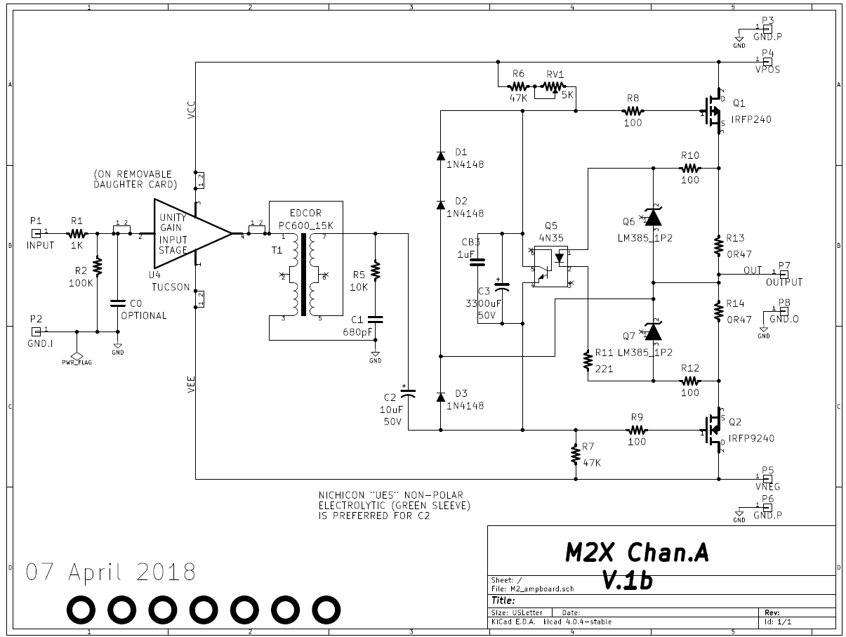
As far as I can tell, there's a signal transformer in the way... 
I can tell you from experience that the PCB mounts well and solidly with the 7 mounting holes that were able to be put on the board. It's good! 😎
I can tell you from experience that the PCB mounts well and solidly with the 7 mounting holes that were able to be put on the board. It's good! 😎
Last edited:
As far as I can tell, there's a signal transformer in the way...
You win the prize.
Green == drill holes
White == Front side silkscreen
_
Attachments
Last edited:
Subscribed!
I love the idea of daughter cards.
I am building up an F6 right now with a different phase splitting transformer (Lundahl) and the JFET buffer has been replaced with Ti Kan’s AMB Alpha 24 which allows for variable gain and balanced/single ended inputs.
The biggest difference between the F6 and M2 is the implementation and role of the transformer.
Very nice! Just make sure this all fits on the UMS heatsinks!
Best,
Anand.
not overly critical , but certainly matter of principle to have them as close to gates as possible
I watched a NP amp with more than 2000 of these pr. channel.....as far as I remember. A waste of good components......we could have used them now...... 🙂
That was 1,176 Jfets per channel, and recall that I kept the leads on
them nice and long for easy re-use by future generations.
And matched!
😛
When member 6L6 powered up his M2x the first time, he and I watched the ammeter on the 115VAC mains (USA). Starting from zero milliamps, it slooooooowly crept up over the span of about 20 seconds or so. Would anyone care to guess why? Hint: the answer is found on the amplifier board, not the power supply board.
_
_
Last edited:
That was 1,176 Jfets per channel, and recall that I kept the leads on
them nice and long for easy re-use by future generations.
And matched!
😛
How many Jfets does one have to keep in stock to get that many matches?
😀
- Home
- Amplifiers
- Pass Labs
- The diyAudio First Watt M2x