If C11/C13 were bad the LEDs wouldn't be illuminating, they are all fine.
I can't get at the bases of TR1 and TR3 directly due to the coupling of the TRs with the LEDs, these voltages were measured at the LEDs.
I can't get at the bases of TR1 and TR3 directly due to the coupling of the TRs with the LEDs, these voltages were measured at the LEDs.
My MOSFET250 amp (the elder sibling of DR. White's designs) developed a fault similar to this due to misadventure on my part with fast opamps. After a long time and changing out quirt a few components I realized the issue was a "blown" capacitor after the shunt reg.
Hopefully you can track down the fault and get the amp working. These amps sound nice when modded as per Dr. White's suggestions.
The MOS250 uses a TL431 instead of the simple zener shunt of the MOS100 and MOS125 amps. That's a simple upgrade as well.
-Raja
Hopefully you can track down the fault and get the amp working. These amps sound nice when modded as per Dr. White's suggestions.
The MOS250 uses a TL431 instead of the simple zener shunt of the MOS100 and MOS125 amps. That's a simple upgrade as well.
-Raja
Remove opamp from bad channel and re measure. Use lightbulb in case something is seriously amiss there.
Ground the input of the op stage in case that worries you. Junction of r7 and r8.
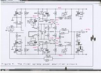
The good amp has this point at 0.19v. The opamp in the bad channel has it much higher but we need to find out why. The first step is to find out if the problem is in the op stage so we need to measure it without the opamp feeding it with 3.5v dc
The good amp has this point at 0.19v. The opamp in the bad channel has it much higher but we need to find out why. The first step is to find out if the problem is in the op stage so we need to measure it without the opamp feeding it with 3.5v dc
The bias is unstable in this conguration, as it is with the op-amp in circuit.
It starts at around 300mA and slowly decays to about 30mA, it's still decaying as I switch it off after testing.
It starts at around 300mA and slowly decays to about 30mA, it's still decaying as I switch it off after testing.
Looks like you clue is the voltage you're seeing at the base of tr5... Worth trying to figure out why its so high. I'll look at the schematic a little more tom but looks clear that this is the area of interest.
I'm starting to suspect TR5 or TR7, both are unobtanium.
I could replace outputs with BUZ900 / BUZ905.
Back in the days of the 2SK133 / 2SJ35 (is that right), Dad is telling me that he had a few failures of these devices due to poor handling.
I could replace outputs with BUZ900 / BUZ905.
Back in the days of the 2SK133 / 2SJ35 (is that right), Dad is telling me that he had a few failures of these devices due to poor handling.
Last edited:
Hi Katie, I may be missing something, but I would have thought that taking the opamp out of circuit pretty much eliminates the feedback path and outputs as the cause of the problem.
I'm not that familiar with the failure mode of transistors like whether it is likley in a failure current could flow from collector to base, which would need to be the case if the problem is with TR5 I would think.
For that reason I would say the most likely suspect is TR3. If it is turning on more than it should then I would think you would be seeing a higher voltage at it's collector due to the resistive divider of R8 and R9. It's obviously not shorted or you would be seeing a higher voltage at the collector and R8 and R9 would probably be burning up.
I'm not sure how the bias circuit with VR1, R11 and TR2 works but I'd check all of those components as well, both for dry joints and for nominal values (and for hfe in the case of the transistor).
Also check the joints on R8 and that you have approx 430 ohms from the collector of TR3 to ground assuming bias pot is set roughly midpoint. The range should be about 400 - 440 depending on the position of the pot, if I've done my calculations properly 🙂 check against working channel for comparison.
Tony.
I wonder what grief might have befallen the amplifier if the -ve 53V wasn't making contact correctly ?
I wonder, can I just remove R18 and R21, the gate stoppers to check that the Outputs aren't leaking or would I need to bias them off ?
Well you could remove tr4 and tr5 and thus simultaneously determine whether the fault is with the "leaky output fet"
or if it is closer to the driver.
If you went down this route you would not need to bias the mosfets off since they are tied to their sources already.
or if it is closer to the driver.
If you went down this route you would not need to bias the mosfets off since they are tied to their sources already.
I wonder, can I just remove R18 and R21, the gate stoppers to check that the Outputs aren't leaking or would I need to bias them off ?
since you're very keen to try this, I'd suggest wiring the gates shut by connecting the gate pins to the source of the respective output fets.
Katie, can you explain what mechanism would result in -6.26V on the base of TR5 if TR7 is the problem component, taking into consideration that it can't be through the feedback path because the opamp has been removed?
I'm not saying it can't (there may be something I don't understand) but I can't see any logical explanation for this. The only path that I can see is reverse through the base tr5 (which would require TR5 to be seriously faulty) or even more remotely through the base of tr4 😕
Tony.
I'm not saying it can't (there may be something I don't understand) but I can't see any logical explanation for this. The only path that I can see is reverse through the base tr5 (which would require TR5 to be seriously faulty) or even more remotely through the base of tr4 😕
Tony.
- Status
- Not open for further replies.
- Home
- Amplifiers
- Solid State
- The David N.J.White 100W MOSFET amplifier