0.1 ohm 3W means 5.5A per resistor or Mosfet, so turn on bias current must be very high for a moment.
The blowout only seems to occur only when using the two pole transitional compensation so im giving up on it. Too bad... Im blaming violent oscillation at startup. Back to two pole compensation again.
I swapped out all ceramic compensation caps for C0G 200V ones. Kemet Goldmax MLCC's. The ones I was using before were of unknown type and voltage rating and got them from college.
I also swapped out the feedback resistors for dale CMF 0.5W 25ppm/C. 4k53 and 261 ohms 0.1% tollerance.
Further more I changed the input filter from 390pF and 1K5 to 330p and 1K8. Just to lower input capacitance a bit.
Somewhere in these changes stability was compromised. When powering up with my lab supply limited to 1A i get high current oscillation and to voltage wont rise. Limiting at 1.3A this doesnt happen and all is fine.
I dont see a chance in transience behaviour or in distortion measurements. All voltages measure correct values. Im not sure why im having these labsupply powerup issues now. Powering from toroidal and recitfier there seems to be no change.
What do you think?
Much cheers and thanks,
Ruben

Excellent work, watching with interest.
Just wish people would stop using Faston-type terminals on PCBs. 🙁
Just wish people would stop using Faston-type terminals on PCBs. 🙁
The culprit has been found. C14 was removed because I suspected it caused destructive bias surge. After soldering it back in there was no more funny startup behavior with current limited bench supply. C14 does indeed cause somewhat of a bias surge but nothing deal breaking. Its there originally to avoid cross-conduction and give better square wave response but apparently it helps with stability before the supplies have charged to full voltage.

Tomorrow I will start construction on a second channel. Very excited to listen to this in stereo.
Cheers!
Tomorrow I will start construction on a second channel. Very excited to listen to this in stereo.
Cheers!
Thank you! what pcb connector do you recommend? I used screw terminals before. I like faston better since Im connecting and disconnecting all the time.Excellent work, watching with interest.
Just wish people would stop using Faston-type terminals on PCBs. 🙁
Molex Mega-Fit connectors with gold-plated contacts are very nice. The Neurochrome products tend to use a lot of those.
I drew blood (and damaged a nearby pin header) last week with a Faston 🙁
I drew blood (and damaged a nearby pin header) last week with a Faston 🙁
The Mega-Fits are nice, but are large and bulky. The Fastons are not ideal but IMO a good compromise between small size, ease of use and price. Direct soldering is not an option for me, none of my builds have ever had the lid closed and not touched or modified again 
PCB screw terminals work too. Tin- or nickel-plated brass work fine and can give a gas-tight connection when tightened properly (just avoid the ones with steel screws). I would personally prefer to terminate the wires in ring terminals when using these.
E.g. https://www.rapidonline.com/keystone-8191-vertical-pcb-screw-terminal-pk10--33-4070
E.g. https://www.rapidonline.com/keystone-8191-vertical-pcb-screw-terminal-pk10--33-4070
MOSFETs cannot produce CFP output structures.
Sometimes no school or software can replace experience.
This is my experience. I told you.
Sometimes no school or software can replace experience.
This is my experience. I told you.
Mosfet CFP sure has many compromises but It is my humble opinion that with this driver and bias circuit it behaves well enough to be worthwhile. However I cannot speak for others.
Last edited:
Pushing for Higher openloop bandwidth.
Still no second channel. I couldn't help myself from pushing the compensation a bit more. Now using the scheme below. This should bring loopgain at 20kHz to about 60dB.
No funny startup business with this amount of 2PC.
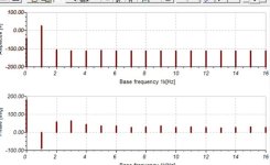
Here are some scope shots:
Testing over-current protection
Next I decided to start testing the over-current protection. It works and shorted output does not damage anything BUT it rings like hell.
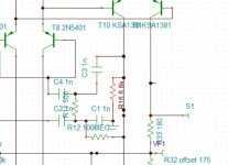
This is the over-current scheme:
This is the output when driving a short (I measured about 0.5Ohms) with R41/54 and C11/2 being 1n and 330R:
Here with R41/54 and C11/2 being 15n and 82R:
It calms down in the up direction but there is no effect in the down direction. Is there a way to calculate the required values based on the oscillation? Spice Simulation does not correlate here. Maybe I have a bad solder joint somewhere which I cant find it. For now Ill try couple different RC values on the pnp limiter.
Much cheers,
Ruben
Spacing parts above the PCB?
So far ive been spacing all components 1mm above the pcb to make it easier to remove them. Now values are finalized, for the next channels I'm thinking of mounting the non-hot components without spacing to the pcb. This will give the build a cleaner look and will save quite some time. However, the top layer hosts the signal ground plane. Perhaps this would increase parasitic capacitance between components and the ground plane.
What is your opinion on spacing the components above the PCB? Only for heat or are these more reasons for doing so?
Thanks!
Ruben
Usually my amotivational syndrome keeps me from making a decision untill I eventually go for the treid and tested method.

Im starting to appreciate the floating components. Even when values are finallized I make mistakes and have to desolder. Each time im glad I left some leadspace to aid this process.
Im starting to appreciate the floating components. Even when values are finallized I make mistakes and have to desolder. Each time im glad I left some leadspace to aid this process.
H
HAYK
What do you think of this mod.
If I liked Chatharsis because it uses autobiased CCS instead of current mirrors. Long time ago I tested the sound that comes out of the mirrors, I never liked it. Still the output VAS has a mirror that I eliminated by transforming the emitter followers into phase splitters. I also changed the feedback network into Dudeck style to eliminate the electrolytic capacitor.

If I liked Chatharsis because it uses autobiased CCS instead of current mirrors. Long time ago I tested the sound that comes out of the mirrors, I never liked it. Still the output VAS has a mirror that I eliminated by transforming the emitter followers into phase splitters. I also changed the feedback network into Dudeck style to eliminate the electrolytic capacitor.
Usually my amotivational syndrome keeps me from making a decision untill I eventually go for the treid and tested method.
View attachment 1194350
Im starting to appreciate the floating components. Even when values are finallized I make mistakes and have to desolder. Each time im glad I left some leadspace to aid this process.
Ants everywhere.
Now thats a unique VAS topology! Nice to push-pull. I really like it. I tried it in LT spice with the simulation of the current pcb version. It appears to allow for larger vas bias current and higher slewrate without much of a IMD penalty. I gives a larger 2nd harmonic (and more THD) however its no longer 180 degrees out of phase.What do you think of this mod.
If I liked Chatharsis because it uses autobiased CCS instead of current mirrors. Long time ago I tested the sound that comes out of the mirrors, I never liked it. Still the output VAS has a mirror that I eliminated by transforming the emitter followers into phase splitters. I also changed the feedback network into Dudeck style to eliminate the electrolytic capacitor.
View attachment 1196009
I encourage you to breadboard this. Let us know how it behaves.
Much cheers,
Ruben
H
HAYK
H
HAYK
I tried the IPS with a constant 8v cascode and with modulated by T15 in the circuit post 114, I get exactly the same result. What does it serve for?
H
HAYK
With my version, I always get higher distortion when I modulate the base voltage, whether constant gate drain or source drain. I only found the the minimum distortion with BF862 is with 6.8v zener. By readjusting the compensation capacitors, I get 0.00016% at 20khz 14vp. Note that I have a monstrous 114db NFB.
Attachments
- Home
- Amplifiers
- Solid State
- The Catharsis Music Magnifier, The Elusive Hexfet CFP from spice fantasy to PCB