amnesis lib
Hi Max,
since .lib files can not be attached I zipped my amnesis2.lib.
May be there is a problem when unzipping.
Here are the 2 models that you can add to your own lib file.
---------------------------------------------------------------------------
.model 2sj103 PJF(Beta=2.197m Rs=76.76 Rd=76.76 Betatce=-.5 Lambda=735.3u
+ Vto=-2.037 Vtotc=-2.5m Cgd=18.95p M=.5045 Pb=.3905 Fc=.5
+ Cgs=17.02p Isr=38.48f Nr=2 Is=3.848f N=1 Xti=3 Alpha=10u Vk=100
+ Kf=1E-18 Af=1)
.model 2sk246 NJF(Beta=1.07m Rs=56.76 Rd=56.76 Betatce=-.5 Lambda=2.8m
+ Vto=-2.638 Vtotc=-2.5m Cgd=10.38p M=.4373 Pb=.3905 Fc=.5
+ Cgs=6.043p Isr=112.8p Nr=2 Is=11.28p N=1 Xti=3 Alpha=10u Vk=100
+ Kf=1E-18 Af=1)
------------------------------------------------------------------------------
Let me know if it works.
Cheers
Thanks.
Yes. I tried to explain that I cannot edit .lib files on this particular PC. I am at work n°2 at the moment. I have to try it on other PCs.
I can say that, even if the simulations are suspect with the present middle power BJTs on critical places (VAS>>drivers), in various combinations, not always what you would call "technically correct", it is sounding glorious to me...
This morning I listened to some Enescu's Violin and piano sonatas...
I think I now understand them.
Cheers,
M.
Dear Hans Polak,
I have a little question for you...
I don't know if you noticed that some schematics have strange RDRD strings connected in parallel to the bootstrapped outputs?
I discovered by accident that this innocuous looking strings modified the simulations so I gave them a try. To my surprise, they modify the sound (not always for the better) of the amp. Today I connect them only in the case that one mod makes the amp sound too ill-defined and "hoarse". Do you have an idea about what may be going on?
For example (+)PS--7K5--D>I--7K5--D>I--output--D>I--7K5--D>I--7K5--(-)PS.
Thanks very much,
M.
Hi Max,Dear Hans Polak,
I have a little question for you...
I don't know if you noticed that some schematics have strange RDRD strings connected in parallel to the bootstrapped outputs?
I discovered by accident that this innocuous looking strings modified the simulations so I gave them a try. To my surprise, they modify the sound (not always for the better) of the amp. Today I connect them only in the case that one mod makes the amp sound too ill-defined and "hoarse". Do you have an idea about what may be going on?
For example (+)PS--7K5--D>I--7K5--D>I--output--D>I--7K5--D>I--7K5--(-)PS.
Thanks very much,
M.
To be honest, I've no idea what you are talking about.
Maybe you can make a screen copy.
Hans
Hi Max,
To be honest, I've no idea what you are talking about.
Maybe you can make a screen copy.
Hans
Never mind...I checked our last version and it simulates the same...maybe that means it is good and before it was bad. Attached.
BTW, my attemps at simulating the QUAD with the 2sj103 .model available predict catastrophic results. Since in real life the amps at least work, I'm inclined to suspect the .models.
Maybe I should buy some 2N5462...
Cheers,
M.
Attachments
Hi Max,
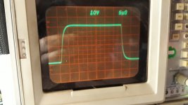
During the last week I made intensive tests with the Quad amp (input stage without Q11/Q12). The amp works stable so far with BD139/BD140 for drivers and boostrapping. For evaluating it is best to use clean 10KHz quare signal (short rise time, no overshot). This is a short abstract of my mayor findings.
DC-Offset
The DC offset is mainly determined by the base current of Q3 flowing into resistor R1=12k. When the Amnesis amp is connected to a source without an input coupling capacitor (which I prefer) the offset depends additionally on the output resistance of the source. When using a source without buffer (e.g. Poti)
the source resistance can vary from 0 to some kiloohms.
Unfortunately the offset and especially the dependancy from the source resistance increases if R33 is increased from 0 to 330 Ohm. In my setup R33<47 is just acceptable. Higher values (>200 Ohm) cause an offset of some volts.
Did you match the transistors esp. the JFET 2SJ103. What value of Idds
have the JFETs you used. The JFETs I used have an Idds of 4..5mA with might be too little??
Input stage
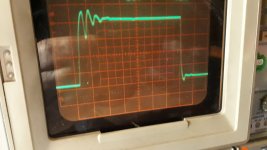
During my tests with 10KHz quare signal an overshot occurs at the amp output which might be the cause for ringing/oscillation.
I finally found out that the overshot is created by the input stage and is depandant
from R33= 0..330 Ohm. Increasing R33 slows the rise time until the overshot disappears. Unfortunately the offset gets worse.
If increasing the input filter R18=1k/C1=1n to slow down the rise time no overshot/ringing occurs at the amp output.
The same is reached when connecting a C=22n between the bases of Q2/Q4
.
I also test the stability of an amp by connecting/disconnecting the input cable
during operation.
The provisions mentioned above stabilize the amp by a great amount.
The question is the influence on sound quality.
More details will follow. Do you have new findings.
Cheers
During the last week I made intensive tests with the Quad amp (input stage without Q11/Q12). The amp works stable so far with BD139/BD140 for drivers and boostrapping. For evaluating it is best to use clean 10KHz quare signal (short rise time, no overshot). This is a short abstract of my mayor findings.
DC-Offset
The DC offset is mainly determined by the base current of Q3 flowing into resistor R1=12k. When the Amnesis amp is connected to a source without an input coupling capacitor (which I prefer) the offset depends additionally on the output resistance of the source. When using a source without buffer (e.g. Poti)
the source resistance can vary from 0 to some kiloohms.
Unfortunately the offset and especially the dependancy from the source resistance increases if R33 is increased from 0 to 330 Ohm. In my setup R33<47 is just acceptable. Higher values (>200 Ohm) cause an offset of some volts.
Did you match the transistors esp. the JFET 2SJ103. What value of Idds
have the JFETs you used. The JFETs I used have an Idds of 4..5mA with might be too little??
Input stage
During my tests with 10KHz quare signal an overshot occurs at the amp output which might be the cause for ringing/oscillation.
I finally found out that the overshot is created by the input stage and is depandant
from R33= 0..330 Ohm. Increasing R33 slows the rise time until the overshot disappears. Unfortunately the offset gets worse.
If increasing the input filter R18=1k/C1=1n to slow down the rise time no overshot/ringing occurs at the amp output.
The same is reached when connecting a C=22n between the bases of Q2/Q4
.
I also test the stability of an amp by connecting/disconnecting the input cable
during operation.
The provisions mentioned above stabilize the amp by a great amount.
The question is the influence on sound quality.
More details will follow. Do you have new findings.
Cheers
Hi dear JOSI1,
Great work as always.
Yes, I was about to post my findings from yesterday. My magnetic vortex experiments kept me busy and entertained for the last weeks...
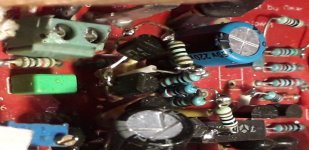
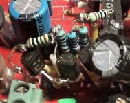
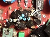
Yesterday I found the time to make the JFET bootstrap for the input CFP. I sacrificed some used 2SJ74 that I had on rest. It should be an easy mod but was very demanding due to my physical execution on the Blame's red PCB.
It worked. A little adjust to the offset is due: it settled around 20mV.
Needles to say that it sounds marvelous to me. The BC556 and the 2SJ74 have only 2.3V to work with.
Now I have to make a confession, which proves how stupid I can be at times. I totally totally forgot to update the initial values of the resistors for the CFP from months ago which were all 1K!!! 😱 No wonder I described the "simple bootstrapped CFP input" as being "dark and heavy on the mid-bass and less detailed" than the other versions. Now the polemic R33 is 248. When I tested 0 versus 330 I found no sound effect. Maybe 100 Ohm is a good starting point.
About your findings and questions. No, I did not match nor measured the J103 😀 I thought you should know me by now, hehe. I imagine the J103 working in bootstrap mode and passing only 3,2mA should work well with only 4mA as Idds...
So it is better to use an active, low impedance source. OK. Maybe Pass' B1 buffer will do?
And you stability tests show that R33 and input filter are good tools to get the amp usable. I don't know about your move about connecting a C=22n between the bases of Q2/Q4. 😕 Never done that.
Remember, I use a parallel (to 68R) pot to reach desired offset, but I never got "some volts" to start with: only mV range.
Anyway. I am very exited about my first listening tests for the new JFET bootstrapped CFP input, and this is listening on youtube with a cell phone 😱 We can stabilize it later 😀
Again, I am very thankful guys for your support and (virtual) confidence in the crazy project of a guy with no background whatsoever in electronics.
Cheers,
M.
PS: I cannot imagine, dear JOSI1, what titanic will force refrains you from testing how it sounds 😀 you must be an ascetic...in my case, anticipation anxiety always wins 🙁
PS2: I don't know what's wrong with the pictures...I'll try to post them later.
Great work as always.
Yes, I was about to post my findings from yesterday. My magnetic vortex experiments kept me busy and entertained for the last weeks...
Yesterday I found the time to make the JFET bootstrap for the input CFP. I sacrificed some used 2SJ74 that I had on rest. It should be an easy mod but was very demanding due to my physical execution on the Blame's red PCB.
It worked. A little adjust to the offset is due: it settled around 20mV.
Needles to say that it sounds marvelous to me. The BC556 and the 2SJ74 have only 2.3V to work with.
Now I have to make a confession, which proves how stupid I can be at times. I totally totally forgot to update the initial values of the resistors for the CFP from months ago which were all 1K!!! 😱 No wonder I described the "simple bootstrapped CFP input" as being "dark and heavy on the mid-bass and less detailed" than the other versions. Now the polemic R33 is 248. When I tested 0 versus 330 I found no sound effect. Maybe 100 Ohm is a good starting point.
About your findings and questions. No, I did not match nor measured the J103 😀 I thought you should know me by now, hehe. I imagine the J103 working in bootstrap mode and passing only 3,2mA should work well with only 4mA as Idds...
So it is better to use an active, low impedance source. OK. Maybe Pass' B1 buffer will do?
And you stability tests show that R33 and input filter are good tools to get the amp usable. I don't know about your move about connecting a C=22n between the bases of Q2/Q4. 😕 Never done that.
Remember, I use a parallel (to 68R) pot to reach desired offset, but I never got "some volts" to start with: only mV range.
Anyway. I am very exited about my first listening tests for the new JFET bootstrapped CFP input, and this is listening on youtube with a cell phone 😱 We can stabilize it later 😀
Again, I am very thankful guys for your support and (virtual) confidence in the crazy project of a guy with no background whatsoever in electronics.
Cheers,
M.
PS: I cannot imagine, dear JOSI1, what titanic will force refrains you from testing how it sounds 😀 you must be an ascetic...in my case, anticipation anxiety always wins 🙁
PS2: I don't know what's wrong with the pictures...I'll try to post them later.
Attachments
Last edited:
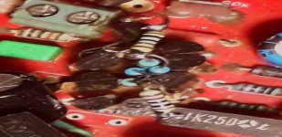
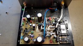
Pics. I hope better ones...and schematic.
Attachments
Last edited:
Hi Max,
I have an itch to listen to the Amnesis amp as soon as possible but
I have just one Amnesis protype available. My present 2way speaker uses
2 amps with a passive crossover network (first order) before the amps.
I have no acceptable speaker (with internal crossover) available at the moment to listen at least in mono mode.
That why I like to order soon some PCBs to get an impression of sound quality.
I upgraded the amp with the new JFET bootstrapped CFP input (2x2 2SJ74BL) and performed my quare wave test. Overshot/ringing has become a little worse but the input filter (1k/1n) solves this problem perfectly.
So could you check at your next listening test if this filter degrades sound quality.
All other proposed measures to stabilize the amp do not work.
2k resistor between sources of the MOSFETs: no influence, C=100n helps a little
10R/100n between bases of driver cascode: a little more ringing
50R/1n from positive base of driver cascode: heavy oscillation
Btw I am using gate stoppers 150 Ohm at both MOSFETs
So increasing the low pass input filter is the only effective measure to improve the stabilty of the amp even at 4 Ohm load and capacitive loads
PS: Did decide which transistors to be used for the driver stage.
Cheers
Code:
PS: I cannot imagine, dear JOSI1, what titanic will force refrains you from testing how it sounds you must be an ascetic...in my case, anticipation anxiety always winsI have an itch to listen to the Amnesis amp as soon as possible but
I have just one Amnesis protype available. My present 2way speaker uses
2 amps with a passive crossover network (first order) before the amps.
I have no acceptable speaker (with internal crossover) available at the moment to listen at least in mono mode.
That why I like to order soon some PCBs to get an impression of sound quality.
I upgraded the amp with the new JFET bootstrapped CFP input (2x2 2SJ74BL) and performed my quare wave test. Overshot/ringing has become a little worse but the input filter (1k/1n) solves this problem perfectly.
So could you check at your next listening test if this filter degrades sound quality.
All other proposed measures to stabilize the amp do not work.
2k resistor between sources of the MOSFETs: no influence, C=100n helps a little
10R/100n between bases of driver cascode: a little more ringing
50R/1n from positive base of driver cascode: heavy oscillation
Btw I am using gate stoppers 150 Ohm at both MOSFETs
So increasing the low pass input filter is the only effective measure to improve the stabilty of the amp even at 4 Ohm load and capacitive loads
PS: Did decide which transistors to be used for the driver stage.
Cheers
Attachments
Hi Max,
I have an itch to listen to the Amnesis amp as soon as possible but
I have just one Amnesis protype available. My present 2way speaker uses
2 amps with a passive crossover network (first order) before the amps.
I have no acceptable speaker (with internal crossover) available at the moment to listen at least in mono mode.
That why I like to order soon some PCBs to get an impression of sound quality.
Haha. I thought you were some sort of monk that could levitate! 😀
Any cheap speaker can serve to have a notion of the potential...think Jehudi Menuhin playing on a modern Chinese violin: you will still get a Master execution...or not.
I upgraded the amp with the new JFET bootstrapped CFP input (2x2 2SJ74BL) and performed my square wave test. Overshot/ringing has become a little worse but the input filter (1k/1n) solves this problem perfectly.
So could you check at your next listening test if this filter degrades sound quality.
All other proposed measures to stabilize the amp do not work.
2k resistor between sources of the MOSFETs: no influence, C=100n helps a little
10R/100n between bases of driver cascode: a little more ringing
50R/1n from positive base of driver cascode: heavy oscillation
Btw I am using gate stoppers 150 Ohm at both MOSFETs
So increasing the low pass input filter is the only effective measure to improve the stabilty of the amp even at 4 Ohm load and capacitive loads
PS: Did decide which transistors to be used for the driver stage.
Cheers
What a beautiful implementation you have there!
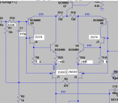
Just to be sure, that would be a "bootstrapped bootstrapped-CFP input", whit J74 inside the CFP and J103 at "the bottom", right?
About ringing, maybe the transconductance of J74 is too high and we shall try other P-JFET inside the CFP.
Did you try a stopper resistor at JFET's gate, like Bimo uses?
Maybe an RC filter at the gate is needed...
Anyway, though the corner F is lowish (+/- 160K), I've seen some reputed amps with that same input filter...I imagine you tried intermediate values also.
I can easily increase series R but // C would more difficult, in order to evaluate sound. Anyway, I am now conducting sound tests with several systems so any mod will have to wait.
BTW, I did not had the time to post that on the next day of the JFET mod, with other source, I had to increase stopper R for the Mosfets from 20 to 130R to avoid oscillatory tendency. I did not (again) do square wave tests, sorry 😱 anticipation anxiety again...
Congratulations on your build and excellent work.
M.
PS: what are your cascoded VAS transistors???
Last edited:
Given the different simulated and real life behavior of JFETs, I've played with LT's own units, which should be well modeled, especially those dual SMD units, and they gave good stability performance. I post extreme values which keep square wave, well...square 😀
I wonder if input impedance can be augmented safely here...I'll check R1.
Maybe single FET (not bootstrapped) CFP will sound OK too...
I never used them nor heard about its "sound" anywhere. Have experience with them?
In fact, those SMD BJTs I used to simulate previously also gave very low noise and good stability. They should withstand thermal stress on low voltage driver position...just saying...
I don't know where to get them nor what the price is.
Summary of Features for the LSJ689A:
Complement to the Ultra Low Noise Monolithic Dual N-Channel JFET LSK489
Ultra Low noise (typically 1.8 nV/Hz @ 1kHz)
Nearly zero popcorn noise
Idss (drain-source saturation current) matching to 10% max
Low offset/tight matching (|Vgs1- Vgs2| = 20mV max)
Low capacitance (Ciss=4 pF)
High input impedance
High breakdown voltage (BVGSS = 40V Min)
Monolithic Dual (2 JFETS on one piece of silicon, better matching and thermal tracking)
Surface mount SOIC-A 8L versions and the smaller SOT-23 6L package
Lead-free/ROHS compliant
Cheers,
M.
Attachments

Last edited:
Hi Max,
LTspice simulation
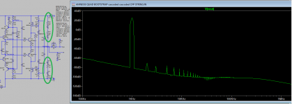
Since last week I am able to run simulations with LTspice.
When using Square wave signal (e.g.10KHz) the simulation never showed an overshot/ringing of the output signal like I determined while testing my prototype. I fear that the simulation is not able to show all the details.
May be you should not rely to much on simulation.
LSJ689A
The only source for ordering I found:
https://store.nacsemi.com/products/detail?part=LSJ689-SOT-23&stock=LIS000000000139
Price is $10.18
no IDDS classification IDDS= -2.5mA ....-30mA: wide spread
Gfs Transconductance 1500 μS: may be a little low
I tried different types even darlington BD679 with no influence on overshot/ringing
Cheers
Given the different simulated and real life behavior of JFETs, I've played with LT's own units, which should be well modeled, especially those dual SMD units, and they gave good stability performance. I post extreme values which keep square wave, well...square
I wonder if input impedance can be augmented safely here...I'll check R1.
Maybe single FET (not bootstrapped) CFP will sound OK too...
I never used them nor heard about its "sound" anywhere. Have experience with them?
In fact, those SMD BJTs I used to simulate previously also gave very low noise and good stability. They should withstand thermal stress on low voltage driver position...just saying...
I don't know where to get them nor what the price is.
LTspice simulation
Since last week I am able to run simulations with LTspice.
When using Square wave signal (e.g.10KHz) the simulation never showed an overshot/ringing of the output signal like I determined while testing my prototype. I fear that the simulation is not able to show all the details.
May be you should not rely to much on simulation.
LSJ689A
The only source for ordering I found:
https://store.nacsemi.com/products/detail?part=LSJ689-SOT-23&stock=LIS000000000139
Price is $10.18
no IDDS classification IDDS= -2.5mA ....-30mA: wide spread
Gfs Transconductance 1500 μS: may be a little low
BD139 and 2N2222PS: what are your cascoded VAS transistors???
I tried different types even darlington BD679 with no influence on overshot/ringing
Cheers
Given the different simulated and real life behavior of JFETs, I've played with LT's own units, which should be well modeled, especially those dual SMD units, and they gave good stability performance. I post extreme values which keep square wave, well...square 😀
I wonder if input impedance can be augmented safely here...I'll check R1.
Maybe single FET (not bootstrapped) CFP will sound OK too...
I never used them nor heard about its "sound" anywhere. Have experience with them?
In fact, those SMD BJTs I used to simulate previously also gave very low noise and good stability. They should withstand thermal stress on low voltage driver position...just saying...
I don't know where to get them nor what the price is.
Summary of Features for the LSJ689A:
Complement to the Ultra Low Noise Monolithic Dual N-Channel JFET LSK489
Ultra Low noise (typically 1.8 nV/Hz @ 1kHz)
Nearly zero popcorn noise
Idss (drain-source saturation current) matching to 10% max
Low offset/tight matching (|Vgs1- Vgs2| = 20mV max)
Low capacitance (Ciss=4 pF)
High input impedance
High breakdown voltage (BVGSS = 40V Min)
Monolithic Dual (2 JFETS on one piece of silicon, better matching and thermal tracking)
Surface mount SOIC-A 8L versions and the smaller SOT-23 6L package
Lead-free/ROHS compliant
Cheers,
M.
Hi Max,
A few remarks
That you can go as low as 6pF is excellent, showing a great stability margin.
But 30 to 50pF is a good practical value in use.
But than the two Fet's on top of each other. With LTspice they are all exactly the same, which in practice will never be the case.
But despite all being the same there is only 200mV Vds left for the top Fet. In practice you will have to select them and put the highest Idss below.
I also found that the BD139/140 in the Amnesis.lib were strange with a Vbe of only 0.4 Volt, so I replaced them with the BD139C/140C models from your .asc file, so you don't have to put them in your .asc circuits.
The zipped .lib file is added.
Hans
Attachments
Hi,
I answer inside...
I have simulated that double JFET input amp with R1=100K without noticing any ill effects. Am I overlooking something obvious due to my lack of knowledge?
So much to try and so little time...
Cheers,
M.
I answer inside...
Hi Max,
LTspice simulation
Since last week I am able to run simulations with LTspice.
When using Square wave signal (e.g.10KHz) the simulation never showed an overshot/ringing of the output signal like I determined while testing my prototype. I fear that the simulation is not able to show all the details.
May be you should not rely to much on simulation.
Yes, I know. It's a good tool though. And good to learn what I have to learn
LSJ689A
The only source for ordering I found:
https://store.nacsemi.com/products/detail?part=LSJ689-SOT-23&stock=LIS000000000139
Price is $10.18
no IDDS classification IDDS= -2.5mA ....-30mA: wide spread
Gfs Transconductance 1500 μS: may be a little low
This price is obviously way higher than BJT's but probably lower than a couple of J74. I cannot easily test SMD in my copper PCB 🙁 Would it be possible to add SMD capability as an EXTRA feature for the already versatile PCB???
It would be USD$40 for a pair of amps...
BD139 and 2N2222
I tried different types even darlington BD679 with no influence on overshot/ringing
Strange. I though higher transconductance would be more risky in that respect...
Cheers
Hi Max,
A few remarks
That you can go as low as 6pF is excellent, showing a great stability margin.
But 30 to 50pF is a good practical value in use.
Thanks. I am following your advices and tricks 😉 . I simulate a lot of tests, though I not always interpret them correctly 🙁 Anyway, those SMD chips, both JFETs as inputs and BJTs as drivers, simulate well, with very low THD and stability so it would be great to test them in real life...but I know we are asking a lot to JOSI1...
But than the two Fet's on top of each other. With LTspice they are all exactly the same, which in practice will never be the case.
But despite all being the same there is only 200mV Vds left for the top Fet. In practice you will have to select them and put the highest Idss below.
Thanks for reminding us the correct way to proceed. Achieving 200-300mV for Vds shall set them in a more linear, more ideal situation, both in terms of THD and TMD, right?
I also found that the BD139/140 in the Amnesis.lib were strange with a Vbe of only 0.4 Volt, so I replaced them with the BD139C/140C models from your .asc file, so you don't have to put them in your .asc circuits.
The zipped .lib file is added.
OK. Thanks very much.
Hans
I have simulated that double JFET input amp with R1=100K without noticing any ill effects. Am I overlooking something obvious due to my lack of knowledge?
So much to try and so little time...
Cheers,
M.
Last edited:
The only purpose of R1 is to keep the amps output offset under control when no source is connected.I have simulated that double JFET input amp with R1=100K without noticing any ill effects. Am I overlooking something obvious due to my lack of knowledge?
Cheers,M.
The output impedance of the voltage source V3 in parallel to R1 is 0 Ohm, that's why you see no difference.
With Fets you could even go higher, but 100K seems a practical value.
Since you are experimenting quite a lot with the in- and output circuits, have you ever thought of making the middle part a differential VAS ?
I have added an unoptimized example.
Hans
Attachments
Hi Hans,
I like differential VAS topology, and with J FET input the extra gain is probably useful.
But having a current mirror on first stage limits the effectivness, as in this case the signal in base of Q15 is full strenght, but on base of Q3 it's much lower due to low imedance of the input side of current mirror. This is why similar circuits like SymAsym use resistors on first stage. But there are other alternatives to this as show in Bob Cordels book.
Anyway still interested to see where this goes.
Regards,
Symon
Sorry, but that's wrong. Q3 is just as much in action as Q15. It is a full differential pair, just like the input.Hi Hans,
I like differential VAS topology, and with J FET input the extra gain is probably useful.
But having a current mirror on first stage limits the effectivness, as in this case the signal in base of Q15 is full strenght, but on base of Q3 it's much lower due to low imedance of the input side of current mirror. This is why similar circuits like SymAsym use resistors on first stage. But there are other alternatives to this as show in Bob Cordels book.
Anyway still interested to see where this goes.
Regards,
Symon
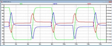
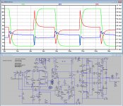
See the collector currents of Q3/Q15 in the image below.
You have now the same symmetrical amount of current for the output stage to pull up as to pull down.
Hans
Attachments
Hi Max,
It really doesn't matter from which side a differential pair is driven.
Either driving one side or both in antiphase sided makes no difference, only the differential voltage is affecting its state.
Hans
It really doesn't matter from which side a differential pair is driven.
Either driving one side or both in antiphase sided makes no difference, only the differential voltage is affecting its state.
Hans
hi Hans,
I think your graph shows that Q3 is recieving a smaller signal amplitude than Q15.
looks like about 20% less, but thats just a rough estimate.
Part of the problem is that hte dynamic impedance of Q10 wired as a diode and diode D10 is low compared impedance of collector of Q13.
I am aware that these impednaces are shunted by the VAS inputs, but the overall effect is that the signal presented is not completely balanced.
Regards,
Symon
Last edited:
Hi Symon,hi Hans,
I think your graph shows that Q3 is recieving a smaller signal amplitude than Q15.
looks like about 20% less, but thats just a rough estimate.
Part of the problem is that hte dynamic impedance of Q10 wired as a diode and diode D10 is low compared impedance of collector of Q13.
I am aware that these impednaces are shunted by the VAS inputs, but the overall effect is that the signal presented is not completely balanced.
Regards,
Symon
No it does not, because as explained above, a differential pair does not care if one side receives less as the other side, only the differential voltage matters.
The real reason why Q15 draws more current has only to do with the Miller cap C10 that has to be charged and discharged each cycle.
Forget all the impedance of Q10, Diode etc.
To show what I mean, I have inserted V2 and V4 in the two lines responsible driving the output transistors.
Now the effect of charging and discharging the Miller cap C10 is no longer part of the current through V2 and V4..
And as you can see, the opposite is now true.
The right side with I(V4) has now greater fluctuations in current as the left side with I(V2), so be careful when trying to coming to conclusions.
See below.
Hans
Attachments
- Home
- Amplifiers
- Solid State
- The AMNESIS amp: a good amplifier, like a gentleman, has no memory.