Peter Daniel said:
This could be really nice package: input stage and 4 output devices on one board. If someone wants more power, they can still use the board as input stage only with additional output separately.
😉
Thanks for the advice, that was my first attempt at an Aleph-X and I will try some more ways to get a more balenced circuit in terms of traces and component placement.
For power, I am initially going to build one channel with 4x1 devices, as specified in Grey's schematic, then if that works, I will move on to a higher powered version. If I wanted to make a scalable pcb, how many 3W resistors would you put in the output stage?
--
Brian
Carpenter,
As of right now tvi's layout looks like the winner, with the mods proposed by hifizen and the Fred's current source (Fred, never say I don't take excellent advice), why not focus on that instead?
At $5 bucks a pop I wouldn't mind buying 1/2 dozen of them. Even if it's just a prototype.
TVI,
I don't understand the spacings for the output resistors, what kind are you using?
Sorry if you have to repeat yourself. I was thinking of playing around with your layout maybe get two pairs per side. Do you mind?
Re: camera ready art

ECD are great. I get all my boards from them. I email them artwork, they ship next day. Like Digi-Key for PCBs. I have gotten line widths down to .007" and they always turn out great.
carpenter said:I'm also working with a local outfit "pcb pro (ECD)". They seem very willing to work with my artwork. I've been able to convert the art to HPGL format. I'll be driving over this morning to see if their pc can read hpgl generated on a Mac.
ECD are great. I get all my boards from them. I email them artwork, they ship next day. Like Digi-Key for PCBs. I have gotten line widths down to .007" and they always turn out great.
BrianGT said:
If I wanted to make a scalable pcb, how many 3W resistors would you put in the output stage?
--
Brian
It all depends on space you have available. Even 3 resistors' spots are fine, because when you piggy back them you end up with 6 and it's about as much as you really need. When settling on 3 resistors don't forget that you can also use different values so that final result is the same.
Now when I started playing with those resistors I finally understood the real reason behind their number. Using the same amount of resistors as the source resistors doesn't create bottle neck situation and limit on the output. I was thinking that using one quality Caddock at 0.1 ohm value was really smart, but when I looked at the diameter of the pins I started to have doubts. Is that where my output currents have to go through? It looks almost like a fuse.😉
grataku said:
TVI,
I don't understand the spacings for the output resistors, what kind are you using?
I was curious about that too.
holding off.....
Does everyone who's shown interest in purchasing pcbs with me want to wait?
John Inlow
Does everyone who's shown interest in purchasing pcbs with me want to wait?
John Inlow
Peter (and possibly Fred),
I am not quite sure if you meant that the output resistors are in large numbers to share the load only or if there was something else. I agree that this might seem like the most obvious reason that they are more than one instead of, as you say, just one small high power resistor. However I would expect the real reason to be, and please forgive my limited knowledge in this area, that they are included in the feedback loop and they will have to be matched to the OPS stage output impedance which AFAIK will roughly will be equal to the source resistors all in parallell if one performs the AC analysis. So for an Aleph 1.2 this will be 7 times 0R47 in parallell giving a 0,067 Ohm output as it has 12+12 times 1.5 giving 1.5/24=0,063 Ohms. For an Aleph 3 having 4 times 0R47 giving 0.118 Ohms output this will match the 2 sets of 0R47 in the output stage giving the exact same 0.118 Ohms. Roughly. I think this the reason and the numbers are what they are in order to reach this match.
Please consider this as unreliable information though...and a guess.
/UrSv
Does everyone who's shown interest in purchasing pcbs with me want to wait?
for me : yes, i would prefer to wait until the freaks and pros made a final design.
A prior comment by Nelson Pass
I was glancing over page one of this thread. If what Nelson Pass says is true, why are we making much to do over nothing?
Page 1. Nelson's quote about Grey's Aleph X design:
"Grey has done an excellent job working this up, and ultimately you will find there are only nominal differences between it and our in-house circuit. As to the sound, I regard the combination of Aleph and Super-Symmetry as giving the best of both designs."
This more I read this sentence, the more I'm certain that I want to continue with my original thoughts. I want that pcb!
This is not to put down the efforts of our in house genius types. They can go on for as long as they like designing improvement after improvement. Without question, they will design the best of the best. In the mean time, I'm certain that Nelson wouldn't have made his statement regarding Grey's design unless he meant every word. And now, I'm ready to continue my quest in earnest.
Thanks for your time,
John Inlow
whoa, lots of new posts again today... let me see... ok:
wessol:
The resistor which should go to negative rail instead of ground is R17 on Grey's original schematic. R21 definitely does have to go to ground!
Adding a 200 ohm variable resistor between the diff pair sources is an interesting idea. To be honest, I've not played around much with mosfet diff pairs, or source degeneration thereof, but I imagine it would work pretty much the same way as with BJTs and JFETs. You will, of course, lose some open loop gain by doing this... the best approach is of course to match the 9610s first, and only then rely on trimming with resistors. Also, any mismatch between the source resistance on each transistor will alter the gain balance. I don't really have much experience with how this will affect the AC operation of the beast. From what I recall reading previously in this thread, knowledgable others seem to feel that leaving the diff pair alone is best... I think the diff pair is probably ok as-is, and matching the 9610s will be sufficient (it may take several in-circuit tries to get the matching right... this is what NP recommends).
Nelson:
Any thoughts on how trimming diff pair current balance with variable source degeneration resistance will affect the non-DC performance aspects of the diff pair? Take, for instance, the situation where the diff pair transistors aren't quite matched, and a little trim in source resistance is used to compensate...
Peter D:
The advantage of running R17 to negative rail instead of ground is two-fold. First, it will be a larger value resistor (almost twice). This is good for rejecting ripple and noise, since the current flowing through it will be generated by a larger voltage across a higher resistance (remember, an ideal current source has infinite impedance). Second, it avoids having supply currents to ground. This prevents DC imbalance between the positive and negative rails, however small it may be. That last point is just a minor nitpick here, but in other circuits it would likely matter more... Nevertheless, the first point remains valid: the CCS will have better performance with this one very simple change, and you shouldn't have to modify and cap values to do it, just the resistor value.
Which reminds me,
tvi:
I recommend you separate the signal ground and supply decoupling ground nodes on the PCB. This way, you can have separate ground wires to a star-point in the chassis, and supply decoupling ripple currents will not mingle with signals. That is, you should have one single, separated ground node on the PCB for R19, R29 and R21 (from Greys original schematic). R1, R4, R44, and R45 could use a common node, or two if it suits the layout. Last, the local supply decoupling caps could share a ground connection, or be separated if convenient for the layout. Otherwise, ground points should not be connected on the PCB, only at the star point.
Also, have you thought about input coupling caps? Maybe these are better to be left off the board, due to the wide variation in mechanical size?
BrianGT:
"NPN compensation capacitors for the output CCSs" <-> "comp. capacitors for main CCSs" Same thing. I guess my language wasn't as clear.
Although none of the circuits people have built so far have required lag capacitors, it never hurts to put the footprint there in case you <i>do</i> need them. Someone is bound to use different transistors, or more of them or whatever, and there's no way to reliably predict for every possible circuit variation if they'll be needed. Better to plan for that rainy day than count on sunshine forever...
The offset resistors Ian contributed are connected between each output and the diff pair source node. Since the diff pair sources will be only a few volts above ground, any negative DC offset in the outputs will pull current from the diff pair CCS, thus reducing current through R23 and R25, and reducing the bias voltage on Q2 and Q11, and correcting the DC offset at the outputs. It's a little feedback loop which operates only on the DC output voltage, and is essentially independant of the signal feedback loops. The smaller the resistors, the more negative feedback is applied, but there's a practical limit to how small you want to make them. I'd try 1k and 4.7k, and compare with no resistors to see what works best. Oh, and this value may need adjusting depending on supply rail voltage.
OK, last item before I go to bed:
I still maintain that the best setup for the diff pair transistors is back-to-back, connected <i>directly</i> to one another with only an insulating pad in between. The goal is good thermal coupling to keep DC output to your speakers minimal as the diff pair transistors heat up and parameters drift. The time constants here can be relatively small (maybe as low as a few seconds) so the better the thermal coupling, the quicker the diff pair can stay balanced. Also, I don't think we should restrict the design by using one particular heatsink which may or may not be available around the world or at in a hobbyists part bin. Using a pair of identical heatsinks sandwiched on either side of the back-to-back diff pairs would be my strong preference. In fact, as wessol mentioned, heatsinks may not even be necessary, depending on your rail voltage...
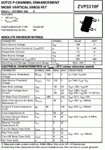
Oh yeah, and I like Fred's current source too... the ZVP3310A should be better suited for use in the diff pair CCS, and something like the LM329 will definitely give lower noise than a zener alone. Great minds do think alike, Fred. 😉
wessol:
The resistor which should go to negative rail instead of ground is R17 on Grey's original schematic. R21 definitely does have to go to ground!
Adding a 200 ohm variable resistor between the diff pair sources is an interesting idea. To be honest, I've not played around much with mosfet diff pairs, or source degeneration thereof, but I imagine it would work pretty much the same way as with BJTs and JFETs. You will, of course, lose some open loop gain by doing this... the best approach is of course to match the 9610s first, and only then rely on trimming with resistors. Also, any mismatch between the source resistance on each transistor will alter the gain balance. I don't really have much experience with how this will affect the AC operation of the beast. From what I recall reading previously in this thread, knowledgable others seem to feel that leaving the diff pair alone is best... I think the diff pair is probably ok as-is, and matching the 9610s will be sufficient (it may take several in-circuit tries to get the matching right... this is what NP recommends).
Nelson:
Any thoughts on how trimming diff pair current balance with variable source degeneration resistance will affect the non-DC performance aspects of the diff pair? Take, for instance, the situation where the diff pair transistors aren't quite matched, and a little trim in source resistance is used to compensate...
Peter D:
The advantage of running R17 to negative rail instead of ground is two-fold. First, it will be a larger value resistor (almost twice). This is good for rejecting ripple and noise, since the current flowing through it will be generated by a larger voltage across a higher resistance (remember, an ideal current source has infinite impedance). Second, it avoids having supply currents to ground. This prevents DC imbalance between the positive and negative rails, however small it may be. That last point is just a minor nitpick here, but in other circuits it would likely matter more... Nevertheless, the first point remains valid: the CCS will have better performance with this one very simple change, and you shouldn't have to modify and cap values to do it, just the resistor value.
Which reminds me,
tvi:
I recommend you separate the signal ground and supply decoupling ground nodes on the PCB. This way, you can have separate ground wires to a star-point in the chassis, and supply decoupling ripple currents will not mingle with signals. That is, you should have one single, separated ground node on the PCB for R19, R29 and R21 (from Greys original schematic). R1, R4, R44, and R45 could use a common node, or two if it suits the layout. Last, the local supply decoupling caps could share a ground connection, or be separated if convenient for the layout. Otherwise, ground points should not be connected on the PCB, only at the star point.
Also, have you thought about input coupling caps? Maybe these are better to be left off the board, due to the wide variation in mechanical size?
BrianGT:
"NPN compensation capacitors for the output CCSs" <-> "comp. capacitors for main CCSs" Same thing. I guess my language wasn't as clear.
Although none of the circuits people have built so far have required lag capacitors, it never hurts to put the footprint there in case you <i>do</i> need them. Someone is bound to use different transistors, or more of them or whatever, and there's no way to reliably predict for every possible circuit variation if they'll be needed. Better to plan for that rainy day than count on sunshine forever...
The offset resistors Ian contributed are connected between each output and the diff pair source node. Since the diff pair sources will be only a few volts above ground, any negative DC offset in the outputs will pull current from the diff pair CCS, thus reducing current through R23 and R25, and reducing the bias voltage on Q2 and Q11, and correcting the DC offset at the outputs. It's a little feedback loop which operates only on the DC output voltage, and is essentially independant of the signal feedback loops. The smaller the resistors, the more negative feedback is applied, but there's a practical limit to how small you want to make them. I'd try 1k and 4.7k, and compare with no resistors to see what works best. Oh, and this value may need adjusting depending on supply rail voltage.
OK, last item before I go to bed:
I still maintain that the best setup for the diff pair transistors is back-to-back, connected <i>directly</i> to one another with only an insulating pad in between. The goal is good thermal coupling to keep DC output to your speakers minimal as the diff pair transistors heat up and parameters drift. The time constants here can be relatively small (maybe as low as a few seconds) so the better the thermal coupling, the quicker the diff pair can stay balanced. Also, I don't think we should restrict the design by using one particular heatsink which may or may not be available around the world or at in a hobbyists part bin. Using a pair of identical heatsinks sandwiched on either side of the back-to-back diff pairs would be my strong preference. In fact, as wessol mentioned, heatsinks may not even be necessary, depending on your rail voltage...
Oh yeah, and I like Fred's current source too... the ZVP3310A should be better suited for use in the diff pair CCS, and something like the LM329 will definitely give lower noise than a zener alone. Great minds do think alike, Fred. 😉
hifiZen
"Although none of the circuits people have built so far have required lag capacitors, it never hurts to put the footprint there in case you do need them. Someone is bound to use different transistors, or more of them or whatever, and there's no way to reliably predict for every possible circuit variation if they'll be needed. But, better to plan for that rainy day than count on sunshine all the time..."
the ZVP3310A : look at surface mount version to include PCB fill area as heat sink. This puppy gets pretty warm.
I move to nominate hifiZen ALEPH commitee chair. He is considering all the right design questions folks.
  No hanging Chads here, and he absolutely has my vote.
So much for staying out of this.
Nil Desperandum,🙁
Fred
"Although none of the circuits people have built so far have required lag capacitors, it never hurts to put the footprint there in case you do need them. Someone is bound to use different transistors, or more of them or whatever, and there's no way to reliably predict for every possible circuit variation if they'll be needed. But, better to plan for that rainy day than count on sunshine all the time..."
the ZVP3310A : look at surface mount version to include PCB fill area as heat sink. This puppy gets pretty warm.
I move to nominate hifiZen ALEPH commitee chair.
He is considering all the right design questions folks. No hanging Chads here, and he absolutely has my vote. So much for staying out of this.
Nil Desperandum,🙁
Fred
ZVP3310A gets pretty hot indeed and it needs bigger heatsink than differencial pair. If you plan to mount differencial pair back to back, a small aluminum plate is all you need. Just figure out the correct spacing between the two FETs.
Oh, and I support Fred's vote.
Oh, and I support Fred's vote.
add some zenerdiodes in series with the drain to lower powerdissipation. this cannot be much noisier than having some one the gates.
Don't mess with Tex X
There is not much votage drain to source as it is with 15V supplies. DO NOT drop voltage here. The capacitance will increase and the output impedance will decrease. I thought this one out and did the modeling. 20-30mA across 5V is 0.1 to 0.15 watts It is not that much dissappation.
  Worry about your output devices instead!
I'm not a real audio engineer but I play one on the web,
Fred
There is not much votage drain to source as it is with 15V supplies. DO NOT drop voltage here.
The capacitance will increase and the output impedance will decrease. I thought this one out and did the modeling. 20-30mA across 5V is 0.1 to 0.15 watts It is not that much dissappation. Worry about your output devices instead!I'm not a real audio engineer but I play one on the web,
Fred
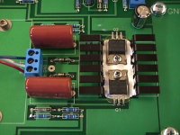
And here's the finished front end board. As you see it doesn't take too many parts to finish it. I didn't use any input caps, no protection zeners, no comp. caps. Just the essential stuff.😉 After I started playing with p2p I don't think I'll ever come back to PCBs, unless of course it will be a production run.😉
Attachments
And that's how it mounts in the amp. Note how output Caddock resistors are connected. The flat pieces of copper (Goertz speaker wire) are used for output buses and Caddocks solder directly to them. The short pieces of the wire coming from Dales connect directly to binding posts.
Attachments

- Home
- Amplifiers
- Pass Labs
- The Aleph-X