Member
Joined 2009
Paid Member
I started building a JLH '69 several years ago including some nice home made pcb's. However, it hit some snags along the way and never got finished. Recently I tested the power supply and found excessive voltage sag under load which leads me to doubt that the transformer is up to the task of a stereo unit so this is going to be a mono block.
The details got spread around in the extensive thread on this topic, starting back in April 2011 [http://www.diyaudio.com/forums/solid-state/3075-jlh-10-watt-class-amplifier-48.html#post2545677] ] and it's hard to keep track of what I was doing so I've opened this thread to capture it and hopefully get the thing finished. Maybe when it's all done the Mods can append this thread to the original monster.
Contraints: I want to use up the bits I have in my junk box and use the half built chasis that I have. This includes all the old RCA 2N3055H's that are rivetted onto the heatsinks. They have date codes spanning 1981 - 1982 (recovered from an e-waste power supply) and I understand they have ft of 2.5MHz. I consider this project a kind of 'industrial archeology', so I won't entertain any notion that these output devices are unsuited. The challenge with older devices is 'beta droop', in other words a significant decrease in input impedance at high current.
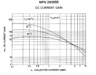
Hiraga's advice was to select devices and operating points so that the dc operating current occurred at the peak of the current gain so that the drop in Hfe with the signal swing would be symmetrical. In any event, it's good advice to avoid operating the devices in a region where beta starts dropping off quickly. The datasheet for 2N3055's puts the peak Hfe at around 200mA at most, especially when hot. With a target idle current of 1.6A we'll need 8 parallel output devices. I just happen to have that number on the heatsinks.
The phase splitter / VAS is TR3 and it's performance has a big impact on the distortion profile and total THD of the amplifier. I will use a better device than JLH had available. I will also consider using a Sziklai (or CFP) compound device for TR3; this suggestion was made by Homemodder in the main thread sometime ago (Feb 2012) and also by Hugh Dean (in private correspondence).
The attached sketch shows the new direction I'm now considering. Whilst it has only a single rail supply, I've 'moved the signal ground' in order to move the output capacitor to a less harmful position - making it resemble a dual rail topology. I think this approach has been tried by others and works well.
The details got spread around in the extensive thread on this topic, starting back in April 2011 [http://www.diyaudio.com/forums/solid-state/3075-jlh-10-watt-class-amplifier-48.html#post2545677] ] and it's hard to keep track of what I was doing so I've opened this thread to capture it and hopefully get the thing finished. Maybe when it's all done the Mods can append this thread to the original monster.
Contraints: I want to use up the bits I have in my junk box and use the half built chasis that I have. This includes all the old RCA 2N3055H's that are rivetted onto the heatsinks. They have date codes spanning 1981 - 1982 (recovered from an e-waste power supply) and I understand they have ft of 2.5MHz. I consider this project a kind of 'industrial archeology', so I won't entertain any notion that these output devices are unsuited. The challenge with older devices is 'beta droop', in other words a significant decrease in input impedance at high current.
Hiraga's advice was to select devices and operating points so that the dc operating current occurred at the peak of the current gain so that the drop in Hfe with the signal swing would be symmetrical. In any event, it's good advice to avoid operating the devices in a region where beta starts dropping off quickly. The datasheet for 2N3055's puts the peak Hfe at around 200mA at most, especially when hot. With a target idle current of 1.6A we'll need 8 parallel output devices. I just happen to have that number on the heatsinks.
The phase splitter / VAS is TR3 and it's performance has a big impact on the distortion profile and total THD of the amplifier. I will use a better device than JLH had available. I will also consider using a Sziklai (or CFP) compound device for TR3; this suggestion was made by Homemodder in the main thread sometime ago (Feb 2012) and also by Hugh Dean (in private correspondence).
The attached sketch shows the new direction I'm now considering. Whilst it has only a single rail supply, I've 'moved the signal ground' in order to move the output capacitor to a less harmful position - making it resemble a dual rail topology. I think this approach has been tried by others and works well.
Attachments
Last edited:
Subscribed.
Have you restricted yourself to using bipolars for the input and voltage amplifier/phase splitter transistors? Assuming you go with the single transistor VA/PS design, a MOSFET in this position could have some useful properties including better buffering the IP from the OP.
Nelson Pass published an interesting variation of the JLH dubbed 'PLH' that uses only 3 transistors, all MOSFETs, and forgoes the input transistor entirely. I think the loop gain of his design is too low for practical use, but the MOSFET VAS/PS applied to your design might give an interesting result.
http://6moons.com/industryfeatures/zen/plh.pdf
HI Bigun !
I like your TGM9 idea .
But I think that you need two equal power (WW) resistor connected between that last two series connected PSU e-lytics caps to achieve good virtual ground reference point , value can be something like 2 x 1K/5W ,
another solution is single 470R/7W res.connected between middle point of that last two series connected e.lytics caps and main transf. secondary coil CT .
BTW , from my experience this type of bipolar PSU with virtual ground need at least few hours for break in time to get stable virtual ground reference point , since brand new PSU e.lytics need time for internal forming to minimise internal current leakage .
I have not read Hiraga nor have I seen this advice.Hiraga's advice was to select devices and operating points so that the dc operating current occurred at the peak of the current gain so that the drop in Hfe with the signal swing would be symmetrical. In any event, it's good advice to avoid operating the devices in a region where beta starts dropping off quickly. The datasheet for 2N3055's puts the peak Hfe at around 200mA at most, especially when hot. With a target idle current of 1.6A we'll need 8 parallel output devices. I just happen to have that number on the heatsinks.
But I do agree that looking at the device hFE vs Ic and fT vs Ic plost in the datasheets is very valuable in selecting suitable operating currents.
I do this for all stages, not just the output stage.
I rarely get up to the peak of either of those plots, the devices would get too hot. But I try to get well up the slope and use Pq as my guide to how far I dare go.
Member
Joined 2009
Paid Member
Have you restricted yourself to using bipolars for the input and voltage amplifier/phase splitter transistors?
I don't have any small signal FETs, only bipolars and I so I plan to build using what I have on hand. Bipolars are 'in the spirit' of the original design but I like to keep an open mind! The option of a CFP VAS would be more linear than any FET of course.
But I think that you need two equal power (WW) resistor connected between that last two series connected PSU e-lytics caps to achieve good virtual ground reference point , value can be something like 2 x 1K/5W
good point! - of course, there may be a tradeoff with speaker-protection here too since no-resistor or a suitably high value resistor will prevent large dc current flow through the speaker in the event of a failure in the output stage.
The Class-A Amplifier Site - Hiraga 20W Class-AI have not read Hiraga nor have I seen this advice.
Attachments
Member
Joined 2009
Paid Member
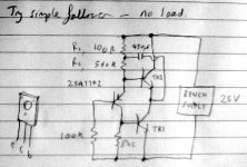
Soak Test
My last attempt at SS Class A ended when the heatsink turned out to be too wimpy [http://www.diyaudio.com/forums/solid-state/159780-biguns-botch-up-amplifier.html ] so this time I want to try it out as soon as possible.
An easy way to do that is a bench supply and a single PNP transistor (2SA1142) front-end, which turns it into a simple voltage follower. I'll bias the base of the input device to the -Ve rail through a 100k resistor which will pin the output somewhere between the rails even if not in the centre exactly. It'll be good enough. The current source (emitter load for the PNP device) will be as per the JLH'69, a 100R in series with 560R (a bootstrap cap isn't necessary but I may wire one in as it'll be needed later).
Attachments
Hi,
I can't follow the logic of 16 output devices per channel at all.
To avoid beta droop and lower output stage input impedance
you just simply kill the output stage input impedance by
reducing it to 1/8 ? * Your busting more than your fixing.
It makes it an entirely pointless version of the JLH for nearly all.
FWIW my favourite "JLH" is the "DoZ" (Death of Zen).
A "JLH" must be simple and minimal, with two ouput devices.
What you can do with lots of output devices in class A is
interesting, but anything sensible won't be near a "JLH".
rgds, sreten.
* It will be less than 1/8, say 1/3 to 1/4, but its a brute
force very inelegant approach to not a major problem.
Last edited:
Member
Joined 2009
Paid Member
the output stage input impedance by
reducing it to 1/8 ?
The input impedance of the upper device, operating as an emitter follower is roughly some capacitance + resistance. The resistance is a reflection of the load via the beta of the device. We are operating at maximum beta, and the parallel devices will each share the current and hence will experience a higher load resistance. Something similar happens in the common emitter configuration too. I don't see any issue there. Of course, at higher frequencies there will be more capacitance to drive. We will just have to live with that. Or have I figured this all wrong ?
Last edited:
Member
Joined 2009
Paid Member
I built up the simple JLH follower point-to-point and hooked it up to a bench supply. At 25V rails it draws 1.55A cold, with about 22mA flowing through the PNP input device. This is a good example of 'using stuff from the parts bin' !
I was able to measure the voltage drop across the 0R15 Re's of the paralleled devices to see on average 195mA per device. The output is sitting at just under 10V so my input bias resistor is bit off from the ideal.
I was able to measure the voltage drop across the 0R15 Re's of the paralleled devices to see on average 195mA per device. The output is sitting at just under 10V so my input bias resistor is bit off from the ideal.
Attachments
Member
Joined 2009
Paid Member
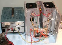
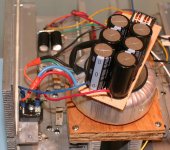
Power Supply
Now that I know the heatsinks are fine and all the power devices work OK the next step is to see if the power supply is going to be OK.
To make sure it was OK to parallel the transformer secondaries I ran a quick test. I wired one wire from each secondary together (in phase), the other outputs I connected together with a 1k2 resistor. The voltage across the resistor was only 7mV (6uA) unloaded which means the two windings have almost identical voltages and they are safe to parallel.
Bridge rectifier was bolted to the chassis with some thermal paste with snubber caps on each diode and an R + C zobel across the output. I roughed up the power supply on perf-board. I used 6 x 10,000uF 50V Nichicon caps from the parts bin and then into two CMC chokes wired as shown in an earlier post. Each choke is 9mH with a dcr of 0R115.
Unloaded I get 27Vdc and 5mVac (rms on my multimeter)
Loaded with 7R8 resistor I get 23Vdc and 99mVac (rms on my multimeter)
This is with around 3A current draw giving me a 4V sag from unloaded. With a 2A bias I should get a solid 24V to driver the amplifier.
Attachments
Last edited:
Hi Bigun, I hope to be proven wrong, however I suspect that power supply is going to prove a little lightweight for this Class A design.
I built a stock-standard JLH on strip board, with a simple power supply not dissimilar to that in your pic and the hum was noticeable (about 100mV measured ripple under load). I had very good results with a capacitance multiplier, unfortunately dealing with the heat dissipation from the pass transistors proved problematic and I ultimately abandoned the experiment (although it didn't sound half bad!). If your experience issues with your simple PSU an extra "LC" for CLCLC might prove beneficial. Good luck!
I built a stock-standard JLH on strip board, with a simple power supply not dissimilar to that in your pic and the hum was noticeable (about 100mV measured ripple under load). I had very good results with a capacitance multiplier, unfortunately dealing with the heat dissipation from the pass transistors proved problematic and I ultimately abandoned the experiment (although it didn't sound half bad!). If your experience issues with your simple PSU an extra "LC" for CLCLC might prove beneficial. Good luck!
It is easier to just temporarily wire the two windings in series AND out of phase.......................To make sure it was OK to parallel the transformer secondaries I ran a quick test. I wired one wire from each secondary together (in phase), the other outputs I connected together with a 1k2 resistor. The voltage across the resistor was only 7mV (6uA) unloaded which means the two windings have almost identical voltages and they are safe to parallel.
Then measure the open circuit voltage across the two remaining open ends.
If the two secondary winding have an identical number of turns then the out of phase voltage will be zero Vac. This also proves the out of phase connections. You are ready to connect for parallel windings.
If the voltage across the open ends measures double the rated voltage then the windings have been wired "in phase". This suits the series connection for a dual polarity supply.
If you want paralleled secondaries, turn one winding around and you now have the correct "out of phase" tappings for parallel connection.
This sounds like you have the R+C snubber on the other end of the PSU from the rectifier/secondary.Bridge rectifier was bolted to the chassis with some thermal paste with snubber caps on each diode and an R + C zobel across the output..................
The R+C snubber should be connected as described for snubbing transformer/rectifier ringing. Not at the other side of the PSU.
Member
Joined 2009
Paid Member
I think you're right there Andrew, the snubber would be better before the rectifier. I think I've seen them afterwards too which is why I went that direction - I haven't done any tests to convince myself that it makes any difference but now that it's all soldered in place I'll probably leave it alone.
Christian - I too am worried about the remaining ripple, that I may have some of the dreaded HUMMMMMMM. My solution maybe to improve the PSRR of the amplifier.
Christian - I too am worried about the remaining ripple, that I may have some of the dreaded HUMMMMMMM. My solution maybe to improve the PSRR of the amplifier.
Since it is a snubber with a damping resistor, it will do no harm where it is.
You could look at adding another at the secondaries if you find you need to attenuate any ringing.
You could look at adding another at the secondaries if you find you need to attenuate any ringing.
Member
Joined 2009
Paid Member
I've been looking more closely at the PSRR of the amplifier, simulated of course. I believe that I can improve the PSRR substantially with the original single rail design, i.e. where the lower rail is held at ground. I believe this is because the lower output power device has it's emitter on that rail and so is sensitive to noise on that rail. The same tricks don't work on the dual rail version I am working towards. I can easily change direction and use an output cap of course. Which is better - it's a tradeoff, between having an output capacitor in the signal vs having less noise from the power supply...
Adding regulation to the main power supply is not an option, there's not enough voltage headroom. I have 60,000uF of caps in there now and I will be increasing this to an effective total of 70,000uF when finished.
Adding regulation to the main power supply is not an option, there's not enough voltage headroom. I have 60,000uF of caps in there now and I will be increasing this to an effective total of 70,000uF when finished.
Member
Joined 2009
Paid Member
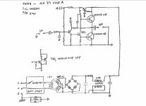
Single Rail Version
With the addition of a a capacitance multiplier in the power rail, between the front end and the output stage we achieve 3 things
i) no voltage limitation on the output stage which can access the full power supply voltage - the input stage can swing high because of the bootstrap
ii) drastically improved PSRR performance of the amplifier
iii) slow turn-on to eliminate the switch-on bump
I'm liking this approach.
Attachments
Looking good. You could use a darlington, or two transistor EF, as the pass transistor to increase the gain and hence the effective 'capacitance'.
Member
Joined 2009
Paid Member
Looking good. You could use a darlington, or two transistor EF, as the pass transistor to increase the gain and hence the effective 'capacitance'.
That's a good point and I think if I were placing the cap multiplier in the power supply to the output stage I'd do just that but a simple Spice simulation shows dramatic improvements in PSRR from just the single device version if used to isolate the front end of the amplifier.
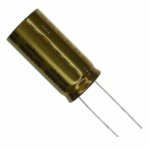
For the 'last cap' in the PSU filter chain and for the output cap I have selected to use the gold coloured caps from Nichicon. Extended listening tests have shown that they provide a clean yet musical tone with extended high frequencies and punchy bass. I hope you didn't believe that BS. I just happen to have some of them on hand. From what I have read there are two precautions that are worthwhile when using output caps, 1) use very large values so that there is negligible ac voltage across the cap (it can't distort the audio if there's no audio across it!) and 2) use a higher voltage rating than you need because this provides for higher quality dielectric oxide interfaces. The caps I have are rated at 50V and 10,000uF each. I'm thinking of using two of them in parallel for the output coupling cap.
Attachments
The other way of looking at this is the HPF formed by the coupling cap. With a 8R speaker load and a 10mF cap it comes out to just under 2Hz - a decade below the audible band, which should minimise LF distortion; a pleasing result. But if that same 8R nominal speaker dips to 4R then the fc is 4Hz; perhaps a little higher than we would like for an electrolytic in the signal path.
I selected 12m for my single rail TGM8 - the largest possible within board constraints. I would have been inclined to go to 22mF (either as a single cap or multiple parallel caps) otherwise.
Those big caps could have fairly high ESR that might influence HF response. Consider putting a much smaller cap in parallel if you're concerned.
Member
Joined 2009
Paid Member
Well I have a few of these gold caps, a couple of them in parallel gives me 20mF. Mine's bigger than yours !
I've read quite a bit about adding a bypass cap - I've seen some interesting measurements on Youtube of all places as well as a lot of well thought out articles. The science doesn't support the need but the golden-ear brigade says otherwise. It's one of the 'those' topics 😀
I've read quite a bit about adding a bypass cap - I've seen some interesting measurements on Youtube of all places as well as a lot of well thought out articles. The science doesn't support the need but the golden-ear brigade says otherwise. It's one of the 'those' topics 😀
Last edited:
- Home
- Amplifiers
- Solid State
- TGM9 - my version of the JLH '69 Class A amplifier