The SKA does not have a VAS. As MIIB I believe that a filter can be put in the input stage to reduce power supply variation injection. My Hiraga has a capacitor bank comparable to a powerful class A/B amp without issue and the Hiraga is a class A.
I am not saying that only CFA amps have good soundstage. I have heard VFA amps with very good soundstage too. But soundstage seems a common characteristic of CFA Amps I (and others) have heard. I am glad to hear that the SKA in VFA has a huge soundstage since it could show great potential 🙂 it is not a question of choosing between VFA or CFA but to build both!
Fab
Last edited:
Member
Joined 2009
Paid Member
Interesting comments about common drain output. Perhaps there is a lot about the sound that is related to this aspect of the topology. The SKA has very good reputation for sound. The Hiraga also. The Pass F5 too. And Rod Elliot's P3A.
In my way of thinking though, the SKA does have a VAS, it is the output stage ! - crazy when you think about it. But in the case of the SKA you can't put a filter on the power rails for the input stage because the PSRR is not limited by the input stage, it is a function of the output stage too, that common drain thing again.
I don't know if I have the time to build both CFA and VFA version - they need a good pcb to do it properly and the topologies would be hard to accommodate on one pcb.
Member
Joined 2009
Paid Member
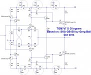
Attached is my simulation file for the VFA and VFA versions. I've tried to set them up so that they are fairly close in operating points but also practical.
I do like the CFA. However, I am getting 6dB worse distortion for 3rd and 5th harmonics. It looks as if the LTP is more linear.
If this isn't what you'd expect - where is my 'error' ?
I do like the CFA. However, I am getting 6dB worse distortion for 3rd and 5th harmonics. It looks as if the LTP is more linear.
If this isn't what you'd expect - where is my 'error' ?
Attachments
In the CFA input you are loosing most of the input bias current through the feedback network, I would separate AC and DC and AC couple the feedback.
Interesting comments about common drain output. Perhaps there is a lot about the sound that is related to this aspect of the topology. The SKA has very good reputation for sound. The Hiraga also. The Pass F5 too. And Rod Elliot's P3A.
In my way of thinking though, the SKA does have a VAS, it is the output stage ! - crazy when you think about it. But in the case of the SKA you can't put a filter on the power rails for the input stage because the PSRR is not limited by the input stage, it is a function of the output stage too, that common drain thing again.
I don't know if I have the time to build both CFA and VFA version - they need a good pcb to do it properly and the topologies would be hard to accommodate on one pcb.
If you consider the output stage of SKA as a VAS then the output stage is the same for the VFA or CFA and they( output stage) suffer the same supply variation. Thus filtering the input stage would improve PSSR of the CFA but surely not as good as the VFA. You mean common source thing....
Yes 2 different pcbs for VFA and CFA would be more appropriate but trying to be as close as possible for the common circuit part....
Fab
Member
Joined 2009
Paid Member
In the CFA input you are loosing most of the input bias current through the feedback network, I would separate AC and DC and AC couple the feedback.
I assume you mean the CCS current is being lost not input bias current - the input bias is just what is needed for the bases of the input devices. The CCS current we can adjust, we can throw it away if we want. The only problem is that as we crank it up we have to use more robust transistors for the CCS. Thing is, just putting in caps to make it an AC coupled feedback doesn't help the distortion. I did figure out it is simply a case of lower OLG. The CFA front end I have used loses gain which I can recover if I further reduce the impedance of the feedback network. In this case I go with the AC coupled approach to avoid high CCS currents. I can get back the gain depending how far I want to reduce the feedback impedance. It directly affects stability though, less impedance makes it faster.
If you consider the output stage of SKA as a VAS then the output stage is the same for the VFA or CFA and they( output stage) suffer the same supply variation. Thus filtering the input stage would improve PSSR of the CFA but surely not as good as the VFA.
It doesn't work - you can't put RC filters between the input and output stage in this topology - if you play with it in spice you'll see that the PSRR can even get worse.
Attachments
...
It doesn't work - you can't put RC filters between the input and output stage in this topology - if you play with it in spice you'll see that the PSRR can even get worse.
I do not use spice but Microcap. Can you do a PDF of your circuit.
Where do you put the filter?
Fab
Member
Joined 2009
Paid Member
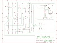
OK - here's an image of a simplified circuit to show where I tried adding RC filters - of course you add them in pairs to both + and - rail. I show 3 locations. None of them work to improve PSRR, and two locations actually make it worse.
Here's why: the input signal comes in from stage left, it's referenced to ground. It is fed to the bases of the input transistors.
All transistors are essentially a voltage controlled device, a differential signal between base-emitter controls current through collector-emitter.
The emitters of the input devices are also referenced to ground through the feedback network. So the input signal modulates the current through the input devices.
This modulated current flows through the collector resistors to generate a voltage across these resistors. This amplified voltage is the difference in potential between the collector of the input transistor and the other side of the collector load, which is the power rail.
So the input pair convert the signal reference from ground over to the power rails. The power rails have essentially become the a.c. 'ground' for the signal at this point in the circuit.
Ignoring the emitter follower buffer for now, the differential signal across the input pair collector loads is applied to the gate-source of the output FETs. The output FET source is also referenced to the power rail. This input signal to the FET modulates the current through the FET and hence through the Drain and into the load. So finally, the signal to once again referenced to ground through the load (speaker).
So where the power rail is acting as a.c. ground for the signal between the input pair and the FETs you can't put a filter in it. If you put an RC filter in the supply rail at this point then any rail noise from the power supply will produce a voltage drop across the R of the filter. This voltage drop will add to the signal a.c. 'ground' between the input pair and FETs. The FETs don't know the difference between the real signal and a voltage drop across the R of a filter. So the rail noise is injected into the output. The PSRR gets worse with a filter.
An RC filter to isolate the current sources doesn't help either since the current sources are already well decoupled from the supply rails. It doesn't cause any harm here though.
Keep going Fab - let's not give up, let's find a way to make this a workable solution or decide we can live with the PSRR as it is ?
Attachments
Last edited:
If you want to get lower distortion and better control over the idle in the output stage i will suggest to mirror the signal into Q4 and Q3. (but what to do with the capacito feed forward...?
Another option could be to make a CFP input, this will lower distortion app 20-30 dB
Another option could be to make a CFP input, this will lower distortion app 20-30 dB
?..
Keep going Fab - let's not give up, let's find a way to make this a workable solution or decide we can live with the PSRR as it is ?
We need R=0 and very big cap 😛
I do not have a big problem with the actual PSSR...
Fab
Member
Joined 2009
Paid Member
Hi MiiB - I think we are OK with output idle current control using the temperature feedback to the CCS. This in turn stabilizes the current flow through the input pair. I think this approach, that Greg uses, is better for this topology than the traditional Vbe multiplier. In my TGM5 I used a Hagerman Vbe multiplier to stabilize the bias despite temperature fluctuations in the VAS current. But in a CFA version of the SKA, the temperature control of the CCS keeps things on track all through the amplifier.
The CFP input is an interesting possibility - but I don't want any more challenges with r.f. oscillations than I have got already. Of course, it could be added, I've made a point-to-point CFP replacement for a VAS transistor before that didn't require any pcb layout alterations - that's in my TGM6.
Hi Fab, yes, it would be quite a large cap!!! Well the place for the RC filter must be in the main power rails.
Hi Bigun...
Hi Fab, yes, it would be quite a large cap!!! Well the place for the RC filter must be in the main power rails.
I think there is no place for any R anywhere on the supply....🙄 except for a very small R in a C-R-C maybe ...then why not a C-L-C...
Do you intend to go back to your adaptation of Greg design for the SKA VFA version and use my thread for the CFA version?
Fab
Member
Joined 2009
Paid Member
Well Fab, I'm a bit undecided whether to stick with the VFA or go with the CFA.
The CFA approach is the flavour of the month on the forum with all the attendant nonsense - I personally doubt there will be any audible difference between the two approaches in the case of the TGM7 (had this been a conventional DX/AKSA/TGM1 type topology I'd say different). They both have very similar OLG and distortion profiles, both with very high gain-bandwidths. With these high feedback factors the differential signal at the error amplifier is small and so both the LTP & Singleton error amplifiers will be operating in a linear region.
However, exploring the two options in Spice has taught me more about the topology, which is fun.
The VFA is proven, with a lot of very satisfied customers. It has a thermally compensated input stage and has good PSRR. However, it has given me some challenges in stability from wiring and pcb layout with few effective tools in the design of the compensation.
The CFA approach offers an alternative compensation scheme, a lower impedance feedback node which will pick up less environmental noise and because it's different from the original GB150 it takes me onto new ground and generally I like that. But it has mediocre PSRR at best. It is also difficult to de-couple adjustment of the dc-offset from adjustment of the idle current, but this is a minor inconvenience.
Any other factors you can think of ?
Last edited:
Member
Joined 2009
Paid Member
Another option could be to make a CFP input, this will lower distortion app 20-30 dB
You planted an idea and although I already passed over that one I came back to it today and ran a simulation of CFA with pair of single devices and CFA with pair of CFPs. There was no difference at all in the distortion profile at 100Hz or 1000Hz. I ran the CFP with 1/3 current through the master and 2/3 though the slave.
Odd, in my current design it offers quite an improvement, bu then again the input pair does not look into resistors but into current mirrors.
how does the CFP pir affect OLG..?? and what about 20 KHZ..??
how does the CFP pir affect OLG..?? and what about 20 KHZ..??
Member
Joined 2009
Paid Member
Hi MiiB, I've attached the spice file for those who are interested. There is no real distortion difference with cfp, at 100Hz, 1kHz and 10kHz with 1.6V input signal playing into 8Ohm linear load.
No it's really not a surprise. If you look at the simulated voltage between base-emitter of the input devices the signal is only +/- 700uV when the input signal is +/-1.6V. There is so much feedback in the amplifier that the error signal at the input pair is tiny. With such a tiny signal the transistors are operating on a very small part of their I-V curve and so are very linear. The CFP brings nothing useful to a party when the linearity is already so good. It does appear to increase the simulated OLG by 2dB, but again, it's small beer when the OLG is very high to start with.
There is no real distortion difference between the CFA and the VFA for the same reason. Perhaps it's only relevant with lower feedback factors. There may be audible differences between the CFA and the VFA for other reasons but it's not clear what they are - perhaps wishful thinking by people who think CFA or VFA are 'better'.
As far as simulations are concerned, the biggest impact on distortion is the bias current through the FETs. Push it up from 100mA per device to 150mA - 200mA per device and the higher order harmonics start falling off rapidly.
Attachments
Last edited:
Member
Joined 2009
Paid Member
OK, now it's time to start-over in Eagle and do a 2nd board. This time I am tempted to include the dc-speaker protect (no input capacitor on the amp remember) and power supply. The question is how to avoid getting the earthing wrong when the end result will be multiple channels ?
p.s. I'm sticking with Greg's VFA approach as I believe it is superior to the CFA option for this topology; PSRR is important.
p.s. I'm sticking with Greg's VFA approach as I believe it is superior to the CFA option for this topology; PSRR is important.
Attachments
Last edited:
Member
Joined 2009
Paid Member
Well, change of heart.
I have made up a schematic with both VFA and CFA options. Depending on which version I want, I simply populate different parts into different locations on the pcb. No power supply or dc protect included but it all fits on the same small pcb as before. I've used considerably wider traces for all high current paths with Quickfit connectors (they are quite popular I notice) for power supply and output. The wiring is simplified, no via's needed for example. I upgraded the main zobel resistor from SMT to a through-hole power resistor and also added separate zobels at the pins of each FET.
For the most part signals are placed above their return current paths. For example, the output currents are routed on the top, whereas the power rails supply to the FETs run underneath them.
In this design the drive signals from the LTP collectors are a.c. referenced to their adjacent power rails. The power rails are effectively the a.c. signal ground for this part of the circuit. So these gate drive traces are routed so that they have a continuous backplane of the respective power rail underneath them.
Overall, traces are shorter so I think it's a better layout than my first version. Assuming I haven't made a booboo somewhere.
Last edited:
...
p.s. I'm sticking with Greg's VFA approach as I believe it is superior to the CFA option for this topology; PSRR is important.
Well, change of heart.
I have made up a schematic with both VFA and CFA options. Depending on which version I want, I simply populate different parts into different locations on the pcb. .....
Hi Bigun
Is it my silence that made you change your mind....😉
All things being equal you should be able to do a fair comparison between the 2 design versions since you have essentially the same layout and parts. However, to be completely fair the CFA will probably need a bigger or better power supply ....
Fab
Member
Joined 2009
Paid Member
- Home
- Amplifiers
- Solid State
- TGM7 - an amplifier based on Greg Ball SKA