Member
Joined 2009
Paid Member
Kean,
Those thermal models are really nice, you should publish those.
About 15 years ago I developed specialized monolithic gold heatsinks for GaAs microwave power devices, specifically to reduce these junction thermal effects. I would have found this type of simulation capability handy to understand circuit behaviour.
I haven't played with the Betsy model (the inductors were all out of place when my Spice opened the file) but I think it would be nice to see more people using realistic load models in their simulations - agreeing on a 'reference' load model might be impossible but that would be the ultimate.
Keep up the good work !!!
I'm sorry, I should have included the inductor model I used.
I wonder if it's possible to use quantum technology to actually teleport heat from the junction into the air... That would be nice, wouldn't it?
I might do some more work on those models before I put them "out there". I want to see if they could be used for MOSFETs. Maybe make some thermistor models... (with thermistors I believe it is possible to compensate for the time it takes to heat up the Vbe multiplier).
It may be hard for people to agree on a load model unless it's fully featured, IE includes the speaker distortion mechanisms at least from a loading standpoint. That would be interesting.
Before we agree on a load though, we need to specify exactly what it is that the realistic model is supposed to reveal about the amp - and which tests should be used with it. I think this is why we still don't use realistic speaker models. No one has taken the idea seriously, and thought it through for its merit.
- keantoken
Unfortunately because LTSpice doesn't support changing the temperature parameter in realtime, temperature simulation as implemented can only be rudimentary. For bipolars and diodes it's passable because transconductance doesn't change with temperature. For MOSFETs this is a big problem.
I just had some success it seems modeling the MUR460 though... Which makes me wonder about those ThermalTrak packages again.
- keantoken
I just had some success it seems modeling the MUR460 though... Which makes me wonder about those ThermalTrak packages again.
- keantoken
keantoken,
The transconductance of diodes and BJTs is inversely proportional to Kelvin temperature. Tkelvin=Tcentigrade+273 so it doesn't change a lot, but it does change. Try testing it with LTspice. Note that transconductace is the change in current for a change in voltage. In other words gm=dIc/dVbe or dId/dVd.
Rick
Member
Joined 2009
Paid Member
I wonder if it's possible to use quantum technology to actually teleport heat from the junction into the air... That would be nice, wouldn't it?
It's possible. If we had SiC transistors, packaged with appropriate materials, we would be able to avoid heatsinks - they would radiate their heat directly (a quantum technique). Researchers have made such devices, that operate whilst glowing red hot. But currently, SiC devices sold as switching FETs aren't packaged to allow them to operate this hot.
The problem with simulating transconductance is that when measuring Ie, this includes currents through parasitic capacitances. With these currents included, trying to vary a voltage source in series with the emitter will create a feedback loop and even if it doesn't cause problems, it will be inaccurate and unreliable at HF. So the only way I could do that would be to reverse-engineer the parasitic capacitance equations and use them to determine how much current is flowing through the junction rather than through capacitance.
- keantoken
- keantoken
Kean... Ever had the thought the the negative tempco of the fets is very close to the opposite of the bipolar's....so a hybrid (fet-BTJ) output stage is possible....like at pair of output laterals drawing 150 mA and with something like 3.3 ohms..to the output.. will perfectly bias multiple sets of output btj's with app 160 mA....and at the same time give a fine thermally balance..
For the prospect of avoiding thermal runaway this may work, but there is still a delay between the heating up of the drivers and outputs, which causes dynamic crossover distortion that varies with power output. ThermalTrak seems to be the current best option in this respect (Unless one gets fancy with an opamp and compensates for this delay, which seems to be possible).
- keantoken
- keantoken
If you look at like the output devices is heating up the drivers then you're right about the thermal delay...but the brilliant thing about this is.. that the drivers is also serving as output devices....thus the reaction is instantly.. and not driven through mass loaded heat-sinks...
Whether the outputs are pre-warmed or not, the thermal transfer delay will be the same. The drivers operate at a much more constant junction temperature, driving only say 50mA into the outputs. The outputs have a widely varying junction dissipation, and if you add to this the thermal resistance between junction and case, and the thermal capacity of the die and case, you'll find that the junction temperature of the outputs is already 15C above that of the drivers before any thermal transfer takes place, in worst-case conditions.
But forget worst-case. How about perfect thermal response, which compensates in real-time (no dynamic crossover) and over long periods of time (stable bias point). And I want to use this on Sankens, not just NJL3281A ThermalTraks.
- keantoken
But forget worst-case. How about perfect thermal response, which compensates in real-time (no dynamic crossover) and over long periods of time (stable bias point). And I want to use this on Sankens, not just NJL3281A ThermalTraks.
- keantoken
Member
Joined 2009
Paid Member
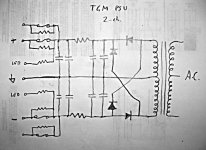
My next step at this time is a proposal to make a Stereo-only version of TGM2, modules mounted to a larger heatsink. For this purpose I'm going to make a new power supply with the same design as my original (used in Home Theatre setup) and same high quality components (ultra low ESR long life 105degC Nichicon filter capacitors for example).
The schematic and first stab at a layout is attached - showing a pcb about the same length as the TGM2 amplifier module itself (shown alongside it).
The schematic and first stab at a layout is attached - showing a pcb about the same length as the TGM2 amplifier module itself (shown alongside it).
Attachments
Member
Joined 2009
Paid Member
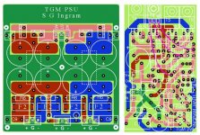
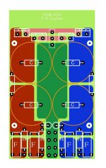
I think a bit more capacitance might be better, so I've redesigned based on some larger caps. This allowed the board to shrink slightly. I have a few SMD chip capacitors I will mount underneath to bypass the large caps.
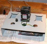
Also made up a test chasis to provide a source of low voltage AC to test that the psu board is working properly after it's made.
Also made up a test chasis to provide a source of low voltage AC to test that the psu board is working properly after it's made.
Attachments
Member
Joined 2009
Paid Member
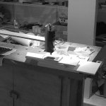
Making the psu pcb. First the iron on toner transfer with ye ole magazine paper, then into the etch bath. I use special ex-Lasagne basins - that way you get to eat and do DIY. I use two of them nested with bottom one full of hot water to make a bath for the top tray full of Ferric Chloride. I recommend chopsticks for dual purpose of stirring and flipping around of pcb during the etch.
Holding up to the light shows fairly clean etching - not perfect but plenty good enough.
Next the toner is removed and it's ready for the drill press - itself a DIY creation.
Progress is made!
Holding up to the light shows fairly clean etching - not perfect but plenty good enough.
Next the toner is removed and it's ready for the drill press - itself a DIY creation.
Progress is made!
Attachments

I love the smell of dissolving copper in the evening!
Experimenting with b&w photography? Adds a vintage, 50's look to the proceedings.
Experimenting with b&w photography? Adds a vintage, 50's look to the proceedings.
I love the smell of dissolving copper in the evening!
Experimenting with b&w photography? Adds a vintage, 50's look to the proceedings.
Might that be muriatic in the morning (like a poor man's napalm) 😀 It seems the m.o.a.n. "thing" is serious business. Us 3 probably churn out more than 1000's of verbose (blah, blah, blah) DIY'ers. 😀. Canadians and Australians seem to build the most and the best. 😎
Another magazine abuser 😎 ... he hee ! FeCl .. too expensive ! My trick is to get the etchant rather hot. (the board below) with minimal etched surface took 140 seconds. Perfect with no pits. Gotta show the 1 pixel hairs on the dog to john ... next "etchfest" (soon). PS's are fun, aren't they... BG ! Big traces , lots of tinning .. making the layout streamlined , big fun. 😉
OS
OS
Attachments
Gotta show the 1 pixel hairs on the dog to john ...
Dude, you should know by now that I'm hard to impress...


No harm in trying though 😀
Member
Joined 2009
Paid Member
Member
Joined 2009
Paid Member
Well that little transformer I set up as a test station was too low voltage to be relevant so I swapped it out for two bigger ones that each generate 30V A.C. - much closer to the final application which uses a 30-0-30.
I didn't wire it up wrong, honest... But I happen to know, that if you accidentally swap the centre tap wire with one of the AC wires when you connect the transformer to your power supply board it becomes a very good voltage doubler and makes the over stressed capacitors quite warm. Of course I didn't do that, but I thought it worth mentioning !
I didn't wire it up wrong, honest...
But I happen to know, that if you accidentally swap the centre tap wire with one of the AC wires when you connect the transformer to your power supply board it becomes a very good voltage doubler and makes the over stressed capacitors quite warm. Of course I didn't do that, but I thought it worth mentioning !Attachments
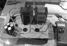
Having more than 2 wires to deal with always confuses me too. If I had a nickel for every time I...🙂
No lab power supply? Worth the time to make one and can be a fun project in itself.
No lab power supply? Worth the time to make one and can be a fun project in itself.
I did that and I also broke my own rule, no bulb in place.But I happen to know, that if you accidentally swap the centre tap wire with one of the AC wires when you connect the transformer to your power supply board it becomes a very good voltage doubler and makes the over stressed capacitors quite warm. Of course I didn't do that, but I thought it worth mentioning !
The only damage was a blown 3886. All the other components were perfect.
Now that you've told me it is a voltage doubler, that explains what went wrong. I will draw it out and see the circuit.
- Status
- Not open for further replies.
- Home
- Amplifiers
- Solid State
- TGM2 amplifier