
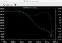
This is what my simulation is saying, with voltage probe insterted into feedback loop at base of feedback transistor in LTP.
I hope you can see what it is that I'm not happy about.
Gareth
I downloaded the file attachment. I have tried to get this to run however I have not be able to get it to display the same image as you - so I have tried some analysis instead.
I have a query about the rearranged circuitry around Q10 which passes 7 m.a. - the bias resistors needing to pass roughly 1.2m.a. to generate that level of current.
R53 is generating a d.c. emitter feedback voltage of roughly 400 m.V. which reduces both the base current for Q10 reducing collector current conduction.
Consequently the bias resistors have to be relatively low in order to pass more current.
The voltage drops across these in comparison with the equivalent resistors in original Naim circuit are higher in static form.
That this will be so in ac form is something to give some serious thought.
Michael
Last edited:
Member
Joined 2009
Paid Member
I have tried to get this to run however I have not be able to get it to display the same image as you
I'm not sure why it would work differently for you, but Spice doesn't save the plotting instructions into the .asc file so you have to create your own plots.
For the bode plot you want to plot the ratio of the voltages at either sides of the voltage source that is inserted into the feedback loop - I put labels on each side of it. Do you know how to do that ? (I usually start by plotting the voltage on the right side of the voltage source with a left-click, then I right-click the name of that signal at the top of the plot window to bring up a dialogue box where you can edit the name of the plot to a formula, for example "V(bode)/V(fdbk)" and then it will apply the formula and display the result).
If you get stuck I can try recreating it and upload the extra file .plt (if I remember correctly) which tells spice what it last plotted and to use the same instructions again.
Could you describe this keystroke process more fully and consider adding it to the beginners LTspice Thread?I....................For the bode plot you want to plot the ratio of the voltages at either sides of the voltage source that is inserted into the feedback loop - I put labels on each side of it. Do you know how to do that ? (I usually start by plotting the voltage on the right side of the voltage source with a left-click, then I right-click the name of that signal at the top of the plot window to bring up a dialogue box where you can edit the name of the plot to a formula, for example "V(bode)/V(fdbk)" and then it will apply the formula and display the result).
If you get stuck I can try recreating it and upload the extra file .plt (if I remember correctly) which tells spice what it last plotted and to use the same instructions again.
Possibly adding a couple of screen captures to show what/where you are referring to?
Member
Joined 2009
Paid Member
I'm not sure why it would work differently for you, but Spice doesn't save the plotting instructions into the .asc file so you have to create your own plots.
For the bode plot you want to plot the ratio of the voltages at either sides of the voltage source that is inserted into the feedback loop - I put labels on each side of it. Do you know how to do that ? (I usually start by plotting the voltage on the right side of the voltage source with a left-click, then I right-click the name of that signal at the top of the plot window to bring up a dialogue box where you can edit the name of the plot to a formula, for example "V(bode)/V(fdbk)" and then it will apply the formula and display the result).
If you get stuck I can try recreating it and upload the extra file .plt (if I remember correctly) which tells spice what it last plotted and to use the same instructions again.
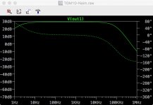
The method I used to change the name of the plot was to click in this area to plot node and feedback voltage.
This will show what changes to the circuit can do but the plots are in negative territory and meaningless without seeing the 0 dB gain point on the vertical axis. I'll give this another shot clicking on the interposed voltage source between these circuit points.
Member
Joined 2009
Paid Member
sometimes I find that you have to tell it to re-scale the plot so that you can see it all. There's an icon at the top of the plot window you can click on to re-scale and ensure it's all visible.
Gareth
I downloaded the file attachment. I have tried to get this to run however I have not be able to get it to display the same image as you - so I have tried some analysis instead.
I have a query about the rearranged circuitry around Q10 which passes 7 m.a. - the bias resistors needing to pass roughly 1.2m.a. to generate that level of current.
R53 is generating a d.c. emitter feedback voltage of roughly 400 m.V. which reduces both the base current for Q10 reducing collector current conduction.
Consequently the bias resistors have to be relatively low in order to pass more current.
The voltage drops across these in comparison with the equivalent resistors in original Naim circuit are higher in static form.
That this will be so in ac form is something to give some serious thought.
Michael
To continue, at a dc level, passing more current through R53 and R54 will increase conduction to some extent in Q10 the increase will be countered by an increase in voltage drop across R52 providing emitter voltage feedback.
This will reduce the base to emitter voltage drop and the base emitter current. Q10 will be working under dynamic conditions where the voltage across R52 will be subject to changing currents and changing voltages.
Under static conditions the network R53 and R54 passes a significant share of the Vbe current which will see-saw in amount with the dynamic action of Q10.
While C7 may bypass some of the effects, the varying voltage across R52 is seen by the collector of Q8. The voltage at that point has an effect on the collector to base capacitance - sucked through the junction and discharged through C17.
However every action has an equal and opposite reaction and Q8 collector is connected to C7 bypass and Q14 phase correction network.
sometimes I find that you have to tell it to re-scale the plot so that you can see it all. There's an icon at the top of the plot window you can click on to re-scale and ensure it's all visible.
Thanks I will look for it. A lot of domestic chores to finish before taking a break away from home next week.
The plot starts and finishes in negative territory passing through 0 dB at 15 kHz and 187kHz with a high point of 20 dB at 52 kHz. No tools are shown in the .raw file.
I am using the LT spice settings recommended see http://www.diyaudio.com/forums/soft...lling-using-ltspice-iv-beginner-advanced.html
Can you point to anything that might need to be changed to get this thing to work.
I am using the LT spice settings recommended see http://www.diyaudio.com/forums/soft...lling-using-ltspice-iv-beginner-advanced.html
Can you point to anything that might need to be changed to get this thing to work.
Member
Joined 2009
Paid Member
Try this instead, I've uploaded a .zip file. Download it and uncompress it to obtain a folder. Inside is an updated spice file and the .plt file which specifies the plot. If you run the spice file inside you should get what you can see in the attached image.
I just realized - I'm running this in a Mac OSX system. It's possible that when run on a PC there are some differences. I'm not sure about that but hopefully the differences will not prevent it working for you. Maybe make sure you have the latest version of Spice.
I just realized - I'm running this in a Mac OSX system. It's possible that when run on a PC there are some differences. I'm not sure about that but hopefully the differences will not prevent it working for you. Maybe make sure you have the latest version of Spice.
Attachments
Last edited:
Try this instead, I've uploaded a .zip file. Download it and uncompress it to obtain a folder. Inside is an updated spice file and the .plt file which specifies the plot. If you run the spice file inside you should get what you can see in the attached image.
I just realized - I'm running this in a Mac OSX system. It's possible that when run on a PC there are some differences. I'm not sure about that but hopefully the differences will not prevent it working for you. Maybe make sure you have the latest version of Spice.
Some software issue is stopping me from making any change to the simulation and saving it.
The closed loop gain of the circuit is 28 or 29 dB.
Changes can bring the simulation gain start high point down to that level - but the phase shift starts at a much lower point as well.
I am not sure what the cause is but it throws doubt over those results.
Member
Joined 2009
Paid Member
That's what I'm seeing tooThe closed loop gain of the circuit is 28 or 29 dB.
Attachments
Member
Joined 2009
Paid Member
Let's Talk Power Supply
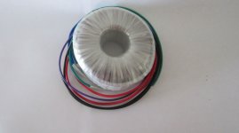
I've ordered me a toroidal power transformer for this project. It's a 200VA donut from Antek.
options...
a) wire the secondaries in series to create a centre-tap, use a single bridge rectifier to create +/-Ve rails to share with both L & R channel (NAP 110)
b) use separate bridge rectifier for each secondary to create a +Ve rail and a -Ve rail, each of which will be common to the L & R channel
c) wire the secondaries in series to create a centre-tap, use two rectifiers with each one creating +/-Ve rails separately for each channel (NAP 140)
Attachments
Last edited:
That's what I'm seeing too
I am not able to post an image of my plot of the .raw file relating to the changes I tried. Some rough figures are:
1.Gain 29 dB 10Hz-20kHz phase -20 degrees
2. 26dB @ 43 kHz -61 degrees
3. 20dB @ 78 kHz -83 degrees
4. 10dB @ 205kHz -95 degrees
5. 0dB @617kHz -102 degrees
6. -37dB @10MHz -210 dgrees
between 0 dB and -37 dB the plots for Gain and phase virtually overlay one another.
Let's Talk Power Supply
You realise the rail voltages of NAP 140 are only 34V and NAP110 even lower? It does make a difference if they are what you intend cloning. If it's the NAP250 with 40V regulated rails you are following, don't try to use unregulated 43V supplies with the VAS transistors specified. I should add that it will work but regardless of additional heatsinking, results will be better if you switch to another clone type, such as an NCC200 clone, and follow that trail of using standard off-the-shelf parts instead.
I would choose (c) if taking the NAP140 route, just for reasons of comparison with other clones pretending to be based on it. I have listened to both models, not in a direct comparison, though I'm sure there won't be a lot of difference with (a) option. There are opinions out there still, about which sounds better but these will probably be irrelevant to your build anyway.
Member
Joined 2009
Paid Member
That's a good point Ian. I don't want to 'fry' the front-end of this amplifier by running it too hot or move the operating points too far from the original.
As you suggest, I've already taken a key element from the NCC200 clone and applied it to my design - the RC rail filters. I will be able to select an operating voltage for the front-end by choosing the resistor values for the rail filters. Not as well controlled as a regulated supply but still with the majority of the benefit.
I will reconsider the values I've posted, perhaps slightly higher values will give me the operating points that are closer to the original circuit with the benefit of better filtering. The output devices will be fine at the higher voltage.
Option a) is certainly the simplest but I can see that option c) is technically better and not much more effort.
Member
Joined 2009
Paid Member
- Status
- Not open for further replies.
- Home
- Amplifiers
- Solid State
- TGM10 - based on NAIM by Julian Vereker