ostripper said:The attachment shows all 3 , 100W -1K...
How did you manage a whopping 0.01% THD at 1kHz with the "Blameless"??
You can use 2n3055/mj2955 for outputs with this topology and reliably get <0.001% THD at 1kHz.
The "Blameless" CM LTP & Miller compensated + EF buffered VAS is definately not a 0.01% THD limiting factor.
Show us how its done, GK.
(I might have done them 3 at 20k , I was tired
but the point was not the total thd,but the distribution
of harmonics.)
At 1-50 watts I agree as I get consistant .001-2% with all 3.
So If you could kindly point out any errata in
my method , the asc's are here...
http://71.203.202.56/pdf1/Electronics/Projects/Audio_amp/Frugalamp/LT_simulations/
OS
Member
Joined 2009
Paid Member
Lumba Ogir said:You won`t regret it. Which type?
These are BYW29E's from NXP which Digikey sell for 70c a piece when you buy more than a few. It adds up to a fair cost for the system but I figure getting better power supply performance is worth it and wouldn't be any cheaper to achieve through better transformer or capacitor design. The next step would be full regulation but I don't want the additional voltage drop or a 'stiff' supply.
These diodes can be heatsunk but I haven't designed them to fit against the 'main heatsink'. Do you think it's worth designing heatsinking for these parts ?
The main heatsink material is Aavid Thermalloy part 68855. If I cut off 3 inch slices for each channel the thermal resistance is around 1.51 degC/W. This isn't a low as what is spec'd for AKSA 55 for example, but for a single channel designed for 25W I am hoping it will be sufficient not to cause a reduction in the lifetime of the output devices ??
Gareth,
You may also want to incorporate some of these parts.
it´s exactly what I have been using. Maybe you could arrange a lighter heatsink for the diodes. I`m not able to assess the main heatsink.These are BYW29E's
You may also want to incorporate some of these parts.
Attachments

Member
Joined 2009
Paid Member
Glen/OS - I'm pretty confident that the topology will yield low enough THD. Along with all the circuits that inspired me it's close to 'book' and therefore low risk. It would be interesting to look at the ratio of H2/3 verses H4+ as a possible indicator of 'subjective listening quality'. I haven't been able to do this with my Spice simulator yet, not sure if I can.
Lumba - I've seen the use of a resistor/cap filter on the output of a PSU but I'm not sure how much incremental gain it allows me. At this point my pcb is 'full' so some clever rework will be needed to add more.
I really need to get an order off to DigiKey as I have nothing at home to start with. I've checked the pcb layout verses the schematic net-by-net and all looks good. Looks like roughly $80/channel but my initial order will have to include some one-off expenses like home-pcb making bits n pieces.
I'm still not sure if I need all the bells and whistles of 'TGM 2' verses the simpler 'TGM 1' so I'm quite looking forward to building this and trying it out...
Member
Joined 2009
Paid Member
Member
Joined 2009
Paid Member

Gareth,
There are not many bells and whistles in v.3.1, nor in this one. Very good THD...I'm still not sure if I need all the bells and whistles of 'TGM 2' verses the simpler 'TGM 1' so I'm quite looking forward to building this and trying it out...
Attachments
Member
Joined 2009
Paid Member
The reason I'm not convinced of the need for the additional circuitry is that the simpler circuit is a close relative of AKSA 55 which has a good reputation. i.e. it may be 'good enough'. But then where's the fun without some experimentation !
I do like the concept of the JFET/BJT input pair because as far as I can see the dynamic range of the JFET is larger - it's linear over a wider range of input voltages compared to the BJT only design. Am I understanding this correctly ?
But the JFET on it's own doesn't have the drive capability for the VAS so we add the BJT to give it some 'back bone'.
Unfortunately I'm still not 100% comfortable with the detailed design calculations for component values. Many of them aren't too critical and a 'feel' for the topology and constraints gives a good guide in most cases. However, too often I am simply 'borrowing' from existing designs without fully appreciating the subtle tradeoffs. For example, some designs use a potentiometer to control the current through the LTP (AKSA/Lifeforce) to influence the dc offset at the output, other designs go straight for the throat and put the pot across the legs of the LTP to adjust balance at the emitters directly. Which is best and why ?
JFETs aren't so easy to source I find, especially matched pairs in a single package, which used to be more common.
Gareth,
JFET input is preferable for every imaginable reason. (Sorry, I`m not explaining why). You could use BC560 until you find some 2SJ74s, which have the same pinout.
This compound (CFP) is more linear than a plain device.
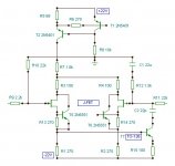
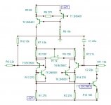
R5 defines the LTP current, 0.7V/68Ohm=10mA and R13/14 the current through T3/T4 in the same manner.
The output DC offset is chiefly caused by imbalances in the LTP.
JFET input is preferable for every imaginable reason. (Sorry, I`m not explaining why). You could use BC560 until you find some 2SJ74s, which have the same pinout.
This compound (CFP) is more linear than a plain device.
R5 defines the LTP current, 0.7V/68Ohm=10mA and R13/14 the current through T3/T4 in the same manner.
The output DC offset is chiefly caused by imbalances in the LTP.
Attachments
You know that Hugh uses CFP in his top of the line amp Soraya, do you?
SK170 is very easy to find and it's cheap if GR grade is OK for you.
SK170 is very easy to find and it's cheap if GR grade is OK for you.
Member
Joined 2009
Paid Member
nelsonvandal said:You know that Hugh uses CFP in his top of the line amp Soraya, do you?
I've not looked at Soraya, all I know is that he named it after his daughter so no doubt he is under pressure to ensure it is his best design or he'll be in hot water !!
Hugh's Lifeforce (successor to AKSA) uses CFP at the input. So does the FrugalAmp from OS. I think Hugh may also have included an emitter resistor in the VAS. Along with other measures the performance is well ahead of the original AKSA from all accounts that I have read. It's more accurate, noticeable improvement in bass. But it's not for sale as a kit and I want to build. Hugh says that the distortion of Lifeforce is way lower, 15dB down from AKSA. People who have upgraded from AKSA to Lifeforce have been very pleased. But it was the unique character of the AKSA that attracted me to it in the first place. The 'limitations' of it's design are what give it this character.
Of course we don't ask Hugh to give up his secrets (well we do, but he says 'no') but I believe from all the reading I've done so far I have an approach:
step 1) build a design with low distortion - TGM2 and TGM3 should achieve this
step 2) allow flexibility at the LTP to affect distortion - primarily though the current balance
step 3) experiment with the compensation - helped along by separating the HF feedback loop (from the VAS) from the LF feedback (from the output).
I have also discovered that the basic circuit topology is common to many other amplifier designs stretching back over many years. Thank goodness we have this forum to help people like me !!!
But I still don't understand enough of the details... 🙄
Member
Joined 2009
Paid Member
p.s. component selection is the other 'art' or 'science' in this process. I don't want to spend big $ on Teflon capacitors for example, but I have tried to pick good components. Electrolytics are Nichicon low impedance 'audio grade', others are polypropylene or mica.
and lastly layout of the pcb. My approach has been...
1/ Check my pcb layout against my schematic net by net.
2/ High current paths have wide traces and high voltage (115V AC) isolated completely at end of pcb
3/ Sensitive input section is put farthest away from high current output stage and power supply
4/ Output section located near power supply so high currents have short distance, including return path. Output is not senstivie to voltage (current mode) so should be safe from pick-up from power supply section which is located next to it
5/ Rectifier diodes kept far away from amplifier, uses soft-recovery diodes to minimize the high-frequency generation during turn-on/off
6/ Single star ground point on pcb for all circuits.
7/ transistor that sets output biass is located next to output transistor to provide negative thermal feedback which will prevent thermal runaway (typical problem with BJT)
8/ negative feedback signal sampled from physical point on pcb which avoids any contamination by the Class AB cross-over current flow due to finite resistance of pcb traces
9/ signal paths at sensitive input stage kept short. Differential input amplfier layout kept symmetrical.
10/ positive power rail to sensitive input stage decoupled via diode and RC filter. Current supply to differential input amplifier regulated with transistor/LED voltage reference.
11/ devices that provide current to drive input capacitance of output stage take their power directly from power supply so not subject to voltage drops along pcb traces to output power devices
12/ no return currents cross other signal paths on the layout
13/ power supply transformer is oriented to minimize projection of flux-leakage onto circuit, uses semi-torroid design with low leakage. Heatsink mounted over back of board provides additional shielding
14/ protection diodes across ground-lift resistor on input in case of high ground currents from small differentials in my house wiring
15/ resistors in parallel with the supply rail fuses prevent large dc at output (which will destroy output load!) in case of one fuse blows
16/ power supply filter uses two parallel caps instead of one large one, improves slew rate
17/ capacitors in signal path polyproplyene (no piezoelectric distortion as with ceramic, low temperature drift)
18/ low resistance-high power resistors in power output circuit are metal film for low inductance (no wire wound)
19/ power devices soldered on back as if surface mount (maximizes contact area for current flow and heat flow) also bolted directly to heatsink
I guess it has to work first time 😎
Member
Joined 2009
Paid Member
I will call the TGM3.1 the JanusTGM (J = Jfet and Janus has two faces, one for +ve and one for -ve input) 😀
All grades of SJ74 can be found at bdent.com but they're a bit expensive.Lumba Ogir said:nelsonvandal,
we need 2SJ74.
The amp could be "mirrored", and SK170 could be used as input transistors. You can buy 100 SK170 for as little as 0.23 Euro/pc.
Member
Joined 2009
Paid Member

Gareth,
However, the high channel resistance (increases with increasing current) leads to large power dissipation and conduction losses. J-FETs have less adequate properties for voltage amplification, especially for handling large voltage swings.
Yes, you are. This is a transconductance stage, where the input is voltage and the output is current, FETs in general make the conversion more accurately. J-FETs are voltage controlled, with the gate-source diode reverse-biased as it should be, there is no current through the gate, giving very high input impedance. J-FETs have much wider operating frequency range than bipolars (warmer sound) and better low-level signal amplifying ability (lower intrinsic noise, the current flows through the channel uninterruptedly, without crossing a PN junction).I do like the concept of the JFET/BJT input pair because as far as I can see the dynamic range of the JFET is larger - it's linear over a wider range of input voltages compared to the BJT only design. Am I understanding this correctly ?
However, the high channel resistance (increases with increasing current) leads to large power dissipation and conduction losses. J-FETs have less adequate properties for voltage amplification, especially for handling large voltage swings.
- Status
- Not open for further replies.
- Home
- Amplifiers
- Solid State
- TGM Amplifier ?