Yes, it works with exactly the same mod list too, except for the LM3886||LM3886 the power decoupling cap size works better at 470u||470u+series element, and the same "outrigger" method can be used as photographed earlier in this thread with the TDA7293||TDA7293, since the only difference is the cap size ("tallboy" skinny Panasonic 50v 470u fits fine for the LM3886 board). Or for a simpler option, some tall skinny Panasonic FC 50v 680u (or higher) caps may do it.
The small other flaws are also, apparent, such as the feedback resistors and feedback-shunt resistors need relocated to a less decorative yet more functional locale, directly at the chips.
And the feedback-shunt coupling cap is too small, as we've seen many times before. However, the LM3886 benefits from a warmer bass harmonic balance, so we won't have to use very very high capacitance for the feedback-shunt coupling cap, like we do on the TDA7293. Probably, the LM3886 board can use 220u~330u size range. It would certainly be easy to get the size right--just pile on multiple 100u till the coupling cap is big enough for non-boomy and clear playback. Yeah, really easy.
So, if someone has already done the TDA7293 parallel board modded as indicated, then getting some performance out of the same designer's LM3886 board, should be quite easy.
The LM3886 Parallel board has dual feedback loops, so if both LM3886's don't pipe up with a SPIKE harmonic distortion and/or noise at precisely the same moment in time, then that noise won't reach the speaker. This LM3886 is usable!
Last edited:
Daniel,
What do you think the usable output is for this dual 3886 board with your modifications you just posted? Let's just say an 8 ohm load since I know those chips are better off driving the higher impedance. What are we talking about, 65 watts @8 ohms @ <10% distortion?
What do you think the usable output is for this dual 3886 board with your modifications you just posted? Let's just say an 8 ohm load since I know those chips are better off driving the higher impedance. What are we talking about, 65 watts @8 ohms @ <10% distortion?
the 3886 is capable of 68W into 8r0 at a lot less than 10% distortion.
A 10% distortion sinewave is so badly distorted when looked at in a scope pic, it cannot be called a sinewave.
Even a 1% distortion looks pretty bad.
I don't have a distortion measuring facility, but I would estimate that a good looking sinewave that is also clear of clipping probably has a distortion of less than 0.5%.
From that, it is my estimate that a 3886 can do at least 68W into 8r0 with less than 0.5% distortion.
Andrew,
I actually have the data sheets on the 3886 and there is no way that a single chip can put out that much power at that distortion level, I think it is really only about 38 watts @ +/- 28v and 50 watts @ +/- 35v and the 50 watts us pushing it and leaning on the Spike protection which will probably be triggered at that level. So how much for two parallel 3886 chips on a common heatsink in that circuit is what I am wondering.
I actually have the data sheets on the 3886 and there is no way that a single chip can put out that much power at that distortion level, I think it is really only about 38 watts @ +/- 28v and 50 watts @ +/- 35v and the 50 watts us pushing it and leaning on the Spike protection which will probably be triggered at that level. So how much for two parallel 3886 chips on a common heatsink in that circuit is what I am wondering.
Read the datasheets again and then build one that approaches the maximum supply voltage.
You will get unclipped outputs that are as National predict.
You will know from my posts that I champion "adequate PSU current capability" as a necessary design target.
I also champion "doubling" the National heatsink guidelines.
Keeping the chip cool and having current capability does allow 65W to 68W into 8r0 from a non regulated PSU that never exceeds +-42Vdc even when mains is at 253Vac.
You will also know that I have described the National chipamps as "current crippled".
I never will use a 4ohms speaker on a chipamp. and thus will never build a bridged version for driving an 8ohms speaker.
A National chipamp cannot properly drive a 4ohms normal sensitivity speaker to norml domestic listening levels.
Design to the limitations of chipamps and they will perform.
Andrew,
I believe that there are ways such as you suggest to coax the most out of the 3386 and the TDA chips but pushing to the limit of output has been stated many times to run up against the Spike protection built into the chips. Now here I was particularly asking about this last board from Ebay with the spacing on that board and running those dual chips? I understand you can increase the heatsink area and increase the heat dissipation rate but those chips are awful close together and I would think that would set a limit as to your actual rate of losses just with the chips heating each other at that distance apart?
I believe that there are ways such as you suggest to coax the most out of the 3386 and the TDA chips but pushing to the limit of output has been stated many times to run up against the Spike protection built into the chips. Now here I was particularly asking about this last board from Ebay with the spacing on that board and running those dual chips? I understand you can increase the heatsink area and increase the heat dissipation rate but those chips are awful close together and I would think that would set a limit as to your actual rate of losses just with the chips heating each other at that distance apart?
You have quoted two values for maximum power output, 38W & 50W, at two supply voltages, +-28Vdc & +-35Vdc
We both know that the 3886 can operate at other voltages.
We both know that if one overloads the 3886 that limiters trigger and ruin the output.
Those triggering points depends on current and voltage and temperature.
Keeping the chip colder by doubling the heatsink delays triggering due to temperature.
Keeping the current lower by never using a 4r0 load delays triggering due to current (into non reactive loads).
Using the highest reliable supply voltage reduces the incidence of voltage clipping.
If I build an amplifier that I know can never exceed a PSU voltage of +-42Vdc, when my mains is at maximum tolerance of 253Vac and test it when mains is at 240Vac, then that is permissible according to National's guidance.
For 68W into 8r0 the amp must put out an unclipped 33.0Vpk
The Vdrop of the amp is approximately the greater of the -ve and -ve values from the datasheet p10. That graph (Clipping Voltage vs Supply Voltage) gives 3V for 8ohms (but actually 8r0 non reactive).
This tells us that the PSU must maintain 33+3V at the supply pins for the duration of the full power test.
If the PSU sags by 2.5V to 3V from the quiescent to full power operation then for the poorer 3V value, the quiescent voltage needs to be +-39Vdc when mains is @ 240Vac. That leaves a margin of safety below the maximum of +-42Vdc when mains is at 253Vac.
The amplifier can give 68W into 8r0 without clipping, from a supply that sags by no more than 3V from a quiescent value of +-39Vdc.
I have tested that situation and find that National's guidance does model this correctly, i.e. 33Vpk into 8r0 when supply is at >+-36Vdc.
This is without clipping and without visible distortion of the sinewave @ 1kHz, which from my earlier post I estimated as distortion less than 0.5%. Maybe a lot less than that.
I do not know if any of these 3886 experimental results would apply to TDA chipamps, nor to other National chipamps
Last edited:
Andrew,
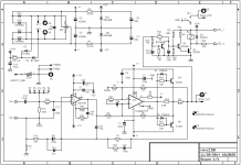
I think you are missing my point here. I am not questioning the ultimate performance of the chips under ideal conditions, they may well perform as specified under those conditions. I have been asking about the particular board shown here from Ebay and in that configuration what the real output level achievable would be with that spacing of the two chip amps on a heatsink? I can't seem to get an answer to that question. We agree on much but you keep avoiding the question that I am asking. I think you statement earlier about never using these chips in a bridged configuration may be what we are looking at on that board, I haven't seen the schematic for the board.
I think you are missing my point here. I am not questioning the ultimate performance of the chips under ideal conditions, they may well perform as specified under those conditions. I have been asking about the particular board shown here from Ebay and in that configuration what the real output level achievable would be with that spacing of the two chip amps on a heatsink? I can't seem to get an answer to that question. We agree on much but you keep avoiding the question that I am asking. I think you statement earlier about never using these chips in a bridged configuration may be what we are looking at on that board, I haven't seen the schematic for the board.
kindhornman:
if i were to use this board and i were less lazy than i actually am, then i would do the physics 101 calculations to determine the case temperatures given a known heatsink and known placement of the LM3886s and the power dissipation i want to get and use the derating curves in the datasheet.
but i am lazy so instead of all that i would use the LM4780 datasheet as a proxy for the actual design. this would be somewhat conservative since two LM3886s placed too close together on a heatsink would still almost certainly be cooler than two LM3886 dies inside one package on the same heatsink.
sfthurber,
You have a better handle on the math for the calculations than I do, I would have to look up everything but as you say because this is a pair of 3886 chips side by side as close as they are now physically placed on that particular board that you would have to derate the output power. Now if you have a fan cooled heat sink then that would be another story.
You have a better handle on the math for the calculations than I do, I would have to look up everything but as you say because this is a pair of 3886 chips side by side as close as they are now physically placed on that particular board that you would have to derate the output power. Now if you have a fan cooled heat sink then that would be another story.
fan cooling only helps a little bit when you have two power chips sharing the same backplate interface.
The added resistance of the interface cannot be negated by external means. The "bottleneck" (Rth j-s) is designed into the package.
Kindh,
what was your specific question that I have obviously missed?
The added resistance of the interface cannot be negated by external means. The "bottleneck" (Rth j-s) is designed into the package.
Kindh,
what was your specific question that I have obviously missed?
The amplifier can give 68W into 8r0 without clipping, from a supply that sags by no more than 3V from a quiescent value of +-39Vdc.
I have tested that situation and find that National's guidance does model this correctly, i.e. 33Vpk into 8r0 when supply is at >+-36Vdc.
This is without clipping and without visible distortion of the sinewave @ 1kHz, which from my earlier post I estimated as distortion less than 0.5%. Maybe a lot less than that.
I have just finished an experimental schematic and layout for a MyRef Rev C derivative with 1x LM3886TF + 2sc5200/a1943 as a Class-B emitter follower. Intended rails are +/- 40V, expected peak swing before clipping is +/- 36 Vp, giving a nominal 80W into 8R (almost double the regular MyRef's 40W).
The LM3886 is not expected to source/sink more than 0.2A in this configuration, so it should effectively keep SPiKe disabled even at relatively high rails of +/- 40V. It should also be possible to use output transistors (Sanken, On Semi) with more robust SOAR and potentially drive 6- to 4-ohm loads comfortably.
The Howland feedback loop as well as the GNFB loop are outside the Class-B power stage, so they will do their bit to contain some of the crossover artefacts, apart from turn-off speed-up diodes connected to each base.
No idea how it will sound, but it can't be worse than just a chipamp + Class-B BJT current-booster, which many people seem to be very happy with.
Attachments
Last edited:
I have just finished an experimental schematic and layout for a MyRef Rev C derivative with 1x LM3886TF + 2sc5200/a1943 as a Class-B emitter follower. Intended rails are +/- 40V, expected peak swing before clipping is +/- 36 Vp, giving a nominal 80W into 8R (almost double the regular MyRef's 40W).
interesting coincidence, i'm working on a nearly identical approach but using dual chipamps (LM4766 and LM4780)
interesting coincidence, i'm working on a nearly identical approach but using dual chipamps (LM4766 and LM4780)
Cool - LM4780 will work for a 2-channel board. I need to check on the maximum supply voltage specs of the LM4766, but IIRC it's quite a bit lower. It's also a bit harder to find locally than the LM3886. TDA7265 is readily available and inexpensive, but supply voltages max out at about +/-30V or lower.
yes, 4766 is a bit lower--
the abs max supply is 74v
http://www.ti.com/lit/ds/symlink/lm4766.pdf
with the bjt outputs into 4 ohms it could get into the neighborhood of 100w per channel
(and have two of them in my parts bin)
the abs max supply is 74v
http://www.ti.com/lit/ds/symlink/lm4766.pdf
with the bjt outputs into 4 ohms it could get into the neighborhood of 100w per channel
(and have two of them in my parts bin)
Last edited:
sfthurber,
You have a better handle on the math for the calculations than I do, I would have to look up everything but as you say because this is a pair of 3886 chips side by side as close as they are now physically placed on that particular board that you would have to derate the output power. Now if you have a fan cooled heat sink then that would be another story.
the thermal physics realities establish diminishing returns fairly quickly whether you use a fan, a taller heatsink, or a wider heatsink. the same is true but to a somewhat lesser extent if you use a thicker substrate heatsinksink or a copper spreader. those things can get expensive enough to make using another board attractive after a certain point. also, note that this board ships with the isolated version (LM3886TF) so the chip's thermal resistance is a bit on the high side with no way around it. the non-isolated version (LM3886T) with a thin mica insulator and appropriate greasing potentially has lower thermal resistance making it easier to cool (if properly installed).
Last edited:
So to mitigate these problems, use the non isolated chip,use separate heatsink remembering that heatsinks have three dimensions. Directly connect the tabs to the heatsink ( remember to isolate the heatsink from Earth/Ground). Use emery/silicon paper to grind both chip tab and heatsink flat. Smear just a smear of heatsink copied. Add a fan if absolutely necessary.
However remember that fans ( like the relays in speaker protection circuits) as an electro-mechanical device the fan may well fail before anything else,
Sent from my iPhone using Tapatalk
However remember that fans ( like the relays in speaker protection circuits) as an electro-mechanical device the fan may well fail before anything else,
Sent from my iPhone using Tapatalk
Meanwhile, back to the TDA7293 Parallel. . .
It is possible to 1), build normally and then 2), set ALL of the chips to slave mode (which leaves them without a small signal voltage amp) and then 3), Add a high quality voltage amp in global negative feedback with the TDA7293 outputs.
An LME driver chip can do a high quality job, and there are many other options for quality voltage amp. Or, perhaps someone would like to drive slave-mode TDA7293 with tubes to make a low cost production tube amp?
I mentioned that option because the LME driver chips are the same brand and have the same clear presentation as the LM3886, but the LME driver chips don't have the screechy tone at all. So, if you wanted an all-chip amp with good performance, that could be an LME driver chip pushing slave-mode TDA7293's.
Basically, it goes this way:
LM3886's Achilles heel is the outputs and spike noise
TDA7293's Achilles heel is the voltage amp.
Well, an LM3886 with no outputs is an LME driver chip. 🙂
And, turning off the TDA7293's voltage amp is done by (first building normally and then) setting slave mode.
And, yes, those chips do work together.
It is possible to build the TDA7293 parallel (as indicated) and then hack the board slightly to set the Master chip into Slave mode. . . and then add an LME driver chip on a little daughtercard.
So, there's LM3886's clarity with TDA7293's prettier tone, in one amp.
- Home
- Amplifiers
- Chip Amps
- TDA7293 Parallel kit from ebay (modular/slave style, no lossy emitter resistors)