Hello,
Recently started a little project where i needed a decent speaker output, so started researching some chip-amp designs.
I landed on a TDA2004 which was readily available from my "local" electronic store. Using the 2005 datasheet for the bridge configuration (the tda2004 datasheet does not have any, but cant really find reason why).
I attach the schematics from the datasheet for reference. Only thing i changed from it was adding a 10k log pot on the input, and using 56ohms instead of 12 to lower the gain somewhat. Should end up at about 38db instead.
I'm very happy with the sound from it, it turned out perfect for my project. Its enough fidelity, hehe.
However, of course I could not let it be, so I found some videos online about using FFT functionality of a oscilloscope to check distortion.
I got interested in this, not mainly for checking the amp as I know there are tons of other checks that needs to be done and as I said, I was happy with the sound.
I just wanted to try out FFT on the scope, as I have never used it before.
I got everything setup and using a .wav file with a 1% distortion added just to check that I'm able to catch that, and I was successful.
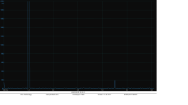
However, I did notice that I have a distortion on the 2khz that is about the same %. Now, it is not in fact the added distortion that is playing tricks here. That distortion is always present, no matter if i choose another 1khz "clean" file or even a function generator.
Did some reading, and I think "crossover" distortion can show up like this. So is this the reason? Can it be fixed on a amp like this? Or maybe is it even expected? I see that there is 1% distortion in the datasheet specs, but not sure if this is what they mean with that.
Please see the spectrum analyzer screenshot and the circuit attached.
Any ideas or other intel is greatly appreciated!


Recently started a little project where i needed a decent speaker output, so started researching some chip-amp designs.
I landed on a TDA2004 which was readily available from my "local" electronic store. Using the 2005 datasheet for the bridge configuration (the tda2004 datasheet does not have any, but cant really find reason why).
I attach the schematics from the datasheet for reference. Only thing i changed from it was adding a 10k log pot on the input, and using 56ohms instead of 12 to lower the gain somewhat. Should end up at about 38db instead.
I'm very happy with the sound from it, it turned out perfect for my project. Its enough fidelity, hehe.
However, of course I could not let it be, so I found some videos online about using FFT functionality of a oscilloscope to check distortion.
I got interested in this, not mainly for checking the amp as I know there are tons of other checks that needs to be done and as I said, I was happy with the sound.
I just wanted to try out FFT on the scope, as I have never used it before.
I got everything setup and using a .wav file with a 1% distortion added just to check that I'm able to catch that, and I was successful.
However, I did notice that I have a distortion on the 2khz that is about the same %. Now, it is not in fact the added distortion that is playing tricks here. That distortion is always present, no matter if i choose another 1khz "clean" file or even a function generator.
Did some reading, and I think "crossover" distortion can show up like this. So is this the reason? Can it be fixed on a amp like this? Or maybe is it even expected? I see that there is 1% distortion in the datasheet specs, but not sure if this is what they mean with that.
Please see the spectrum analyzer screenshot and the circuit attached.
Any ideas or other intel is greatly appreciated!
Thank you for your reply.
Kindly, could you elaborate a bit? What effect would this proposed change have?
And might this affect the problem I have?
Kindly, could you elaborate a bit? What effect would this proposed change have?
And might this affect the problem I have?
Hi!
I'd make some sanity checks on the measurements to try to find the source of this 2nd harmonic distortion.
Just a note: we can see in the diagram below that this is a "low cost" bridge mode, where the signal from the amplifier output on the left is injected in the other amp on the right but configured as inverter amp.
The more high quality bridge mode would create an inverted signal at pre-amp stage, with an op amp, to feed the other amplifier, so it doesn't use a power amp output to feed another power amp.

In order to check if this distortion comes from the bridge mode, I'd make the following tests:
1) Measure the distortion only on the amplifier output on the left (single ended), which receives the signal directly from the source.
2) Measure only on the right amplifier output.
3) Try other frequencies (100Hz, 10kHz) just to make sure it is really a 2nd harmonic and not something else.
4) I'm assuming you measured your audio source first and there is no 2nd harmonic on it, right?
Do you have a differential probe? If not, are your scope isolated from earth?
I normally use a differential pre-amp (simple with opamp) to measure things on bridge amps, since I don't have a differential probe.
I'd make some sanity checks on the measurements to try to find the source of this 2nd harmonic distortion.
Just a note: we can see in the diagram below that this is a "low cost" bridge mode, where the signal from the amplifier output on the left is injected in the other amp on the right but configured as inverter amp.
The more high quality bridge mode would create an inverted signal at pre-amp stage, with an op amp, to feed the other amplifier, so it doesn't use a power amp output to feed another power amp.
In order to check if this distortion comes from the bridge mode, I'd make the following tests:
1) Measure the distortion only on the amplifier output on the left (single ended), which receives the signal directly from the source.
2) Measure only on the right amplifier output.
3) Try other frequencies (100Hz, 10kHz) just to make sure it is really a 2nd harmonic and not something else.
4) I'm assuming you measured your audio source first and there is no 2nd harmonic on it, right?
Do you have a differential probe? If not, are your scope isolated from earth?
I normally use a differential pre-amp (simple with opamp) to measure things on bridge amps, since I don't have a differential probe.
Hey, thanks for your reply.
This might very well be due to the design as you say, I just would like to confirm the reason if so. Or maybe its something else.
Just to highlight, since I'm picking up the 1% distortion added in the wav-file in the correct amplitude and so, I do think the scope is setup correctly and is picking up "the right thing". Just to note further on that, I have both a regular bench-top scope with FFT and a PicoScope (USB-scope) They both indicate the exact same, however, for this I tend to use picoscope as it has a little better interface for the FFT-functionality, at least with my experience so far.
For 1 & 2) please see this image, it is from output 1, and we can clearly see that the distortion is there, (just note, all these is with the added 1% distortion, which is showing up on the correct space).
The output 2 is virtually identical to this, which I hope is expected, or otherwise I'm doing something wrong in the measurement.

3) Ran out of test-leads for this to comfortably hook up the function generator, I will need to get back with this point.
4) Please see this picture from the audio-source. To me it looks clean without that 2nd harmonic and just the added distortion.:

For the other frequency-tests i need to come back. If any other ideas come up, please let me know.
Thanks for your help so far!
This might very well be due to the design as you say, I just would like to confirm the reason if so. Or maybe its something else.
Just to highlight, since I'm picking up the 1% distortion added in the wav-file in the correct amplitude and so, I do think the scope is setup correctly and is picking up "the right thing". Just to note further on that, I have both a regular bench-top scope with FFT and a PicoScope (USB-scope) They both indicate the exact same, however, for this I tend to use picoscope as it has a little better interface for the FFT-functionality, at least with my experience so far.
For 1 & 2) please see this image, it is from output 1, and we can clearly see that the distortion is there, (just note, all these is with the added 1% distortion, which is showing up on the correct space).
The output 2 is virtually identical to this, which I hope is expected, or otherwise I'm doing something wrong in the measurement.
3) Ran out of test-leads for this to comfortably hook up the function generator, I will need to get back with this point.
4) Please see this picture from the audio-source. To me it looks clean without that 2nd harmonic and just the added distortion.:
For the other frequency-tests i need to come back. If any other ideas come up, please let me know.
Thanks for your help so far!
Hello!
Ok! We confirm that your source is clean and only has the controlled added distortion, which is indeed a good idea to control the measurement environment.
We also confirm that the single ended amp already has the 2nd harmonic distortion, so nothing related to the bridge mode, which narrows down the problem.
Thus, we can focus only on the "first" amp and make single ended measurements.
Let me think more about other measurements.
I have a TDA2003 (1x10W) here, which is similar to TDA2004 (2x10W) and later on today I'll measure it to see if it has the same issue.
PS: one thing you can explore in your scope is to show the measurement in dB to better view big (fundamental) and small (harmonics) signals in the same graph. Fundamental will be 0dB and the added distortion (1%) will be -40dB.
Last edited:
Hi,
I made a quick test with the TDA2003 in a protoboard and I noticed that it is very sensible to layout.
So far, I get strong 2nd harmonic distortion when loading it with 4.7ohms and 2Vpeak.
Negative part of sinewave gets distorted.
Without load there is no distortion.
After lunch, I'll play a bit more with this amp to try to clean it up.
It's interesting to check your waveform in time domain with load and without load - see if there is any difference or oscillation.
See results in time and frequency domain (fft).
My scope is based on 8 bits so anything below 48dB has not much meaning.
Hi!
After playing with layout and changing/adding some capacitors here and there and also changing the feedback network to have less gain, I could remove the oscillation and now the amp works fine within the specs (<0.3%).
Check your layout and see in the time domain if there is no high frequency oscillation.
Do you have this TDA2004 already in a PCB or still in a protoboard?
Hello,
Thank you very much for your input and assistance with this, I really appreciate it.
It did not even occur to me to test it without load, that's what you get for your first steps in to audio circuits 😀
But yes, removing the load, the distortion disappear like magic. Using a 4ohm load. Adding screenshot of it without load.
Side-note, I don't really pick up the very noticeable trace on the normal scope view as you do, what % of distortion did you have there?
So about the same experience as you had with your circuit.
That's very cool that you where able to find a way around it. Kindly, could you elaborate a little further on what changes you did?
I actually etched a PCB for the design, so its more or less given currently. But I can of course change any resistors or caps that is in the design i posted above.
Now, I really do not have the experience to know what to change.
I do also have 2x 1000uF caps on the power-line close to the chip, if that also needs a change/addition?
If design it needs to be changed further, I can make a new design. I'm all in for the learning with this!
Attachments
Even harmonics are related to unsymmetric distortion. And this happens with these single supply amps:
The supply current return path superimposes a bit of voltage to input GND - and supply current pulsations
are twice of the fundamental signal frequency. And that is the elephant in the room. Strict, low impedance
gnd layout is your option, nothing else.
The supply current return path superimposes a bit of voltage to input GND - and supply current pulsations
are twice of the fundamental signal frequency. And that is the elephant in the room. Strict, low impedance
gnd layout is your option, nothing else.
Hello!
These devices are critical to oscillation. So carefull PCB design is needed and this is tricky.
As mentioned in the post #10, yes ground is very important. You have to have a single GND point and distribute the other GND connections in a star design.
The best way to go is to use the PCB suggestion found in the datasheet or buy an off the shelf PCB for it.
Take a look on the sinewave in time domain to check if there is no spurious high frequency oscillation.
If you have oscillation, this must be resolved and it is probably the cause of distortion.
In general, these oscillations varies with load and voltage. So you may see a nice 100mV sinewave but when you increase the volume you start to see spurious oscillations. Sometimes in 8ohms works fine and in 4ohms not. You need a very clean sinewave in all situations.
In my case, in the first try, 2nd harmonic was at -25dB, so THD=5.6% considering just the 2nd.
The changes I did were to address the problems found in my protoboard and power supply I used. This doesn't mean it will be applicable to your PCB.
It was just a prove of concept that TDA2003 doesn't have high THD.
Probably I had many parasitic inductances in the wires I used to make the quick test.
In your PCB, you may try different changes.
What you can easily try is to add decoupling capacitors (100nF) on the power supply, in the output etc.
I know it's not easy to find what to change.
If you can take a picture of your PCB, maybe someone can suggest improvements on it.

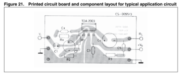
In TDA2004 datasheet we see their suggestion which I'm quite sure works with the typical application circuit.
But this PCB is for single ended not bridge - you may try to use it and after check if it works, make the changes for bridge mode.
You can also use an opamp unity gain inverter to feed one of the amps externally (more high quality bridge mode).

These devices are critical to oscillation. So carefull PCB design is needed and this is tricky.
As mentioned in the post #10, yes ground is very important. You have to have a single GND point and distribute the other GND connections in a star design.
The best way to go is to use the PCB suggestion found in the datasheet or buy an off the shelf PCB for it.
Take a look on the sinewave in time domain to check if there is no spurious high frequency oscillation.
If you have oscillation, this must be resolved and it is probably the cause of distortion.
In general, these oscillations varies with load and voltage. So you may see a nice 100mV sinewave but when you increase the volume you start to see spurious oscillations. Sometimes in 8ohms works fine and in 4ohms not. You need a very clean sinewave in all situations.
In my case, in the first try, 2nd harmonic was at -25dB, so THD=5.6% considering just the 2nd.
The changes I did were to address the problems found in my protoboard and power supply I used. This doesn't mean it will be applicable to your PCB.
It was just a prove of concept that TDA2003 doesn't have high THD.
Probably I had many parasitic inductances in the wires I used to make the quick test.
In your PCB, you may try different changes.
What you can easily try is to add decoupling capacitors (100nF) on the power supply, in the output etc.
I know it's not easy to find what to change.
If you can take a picture of your PCB, maybe someone can suggest improvements on it.
In TDA2004 datasheet we see their suggestion which I'm quite sure works with the typical application circuit.
But this PCB is for single ended not bridge - you may try to use it and after check if it works, make the changes for bridge mode.
You can also use an opamp unity gain inverter to feed one of the amps externally (more high quality bridge mode).
Attachments
If you find high frequency oscillations, try to add 100nF poliester capacitors in parallel with the electrolitycs.I do also have 2x 1000uF caps on the power-line close to the chip, if that also needs a change/addition?
Sure, they are old and today there are much better other amps available.I checked these buggers during the 80s with discouraging results, and trashed them.
But they are very popular, easy to find, cheap etc, specially when you don't have access at a reasonable cost to official distributors such as Mouser, Digikey etc.
If you can resolve the oscillation, they work, if not fakes or not too bad fakes.
Thanks both for your inputs!
This is very interesting for sure.
Now, it looks like our main suspect is GND-design? Been reading up on the ”star ground” layout that seem to be a option. This was not implemented in my current design, so this is for sure a way to improve, if we suspect this could be the culprit?
I think I’m getting some of these spurious oscillations on the sine wave as you are referring to. It’s not very much, but they are there ”moving” the wave around ever so slightly. Difficult to share on a screenshot though. If I understand correctly, this could be caused by not using star ground design?
In your experience, and I do understand it’s difficult to know maybe with the measurements shared so far, but how far off am I currently would you say? Is the distortion shown considered very bad?
I will attempt the capacitor suggestions to see if it has any effect on current design.
Btw, would using a battery to power the circuit temporarily help in diagnosing further?
Also, any tips on a more ”modern” chip that would be easier to avoid these issues with? Would like to aim to not have more external components than what is in current design. As I will have some space constraints later in the build.
PCB is really trick to work with. The "star topology" is a generic orientation so as to have a single GND point and do not allow current flowing through a long track with derivations. In this long derivation, if high current flows, you have non zero voltage along the track (due to the track resistance), which generates spurious signals since this track should be ideally the reference zero volt. This can be the cause of oscillations and also power supply noise (120Hz) if the rectifier is in the same PCB with components connected along the GND track.Now, it looks like our main suspect is GND-design? Been reading up on the ”star ground” layout that seem to be a option. This was not implemented in my current design, so this is for sure a way to improve, if we suspect this could be the culprit?
You can also use another aproach which is the ground plane, where most of the PCB is made by the ground. This is good for shielding, is good cause it has low resistance (a lot of cooper area) but can also cause parasitic capacitances.
Other generic orientation is keep components as close as possible to avoide parasitic inductances.
It's no easy.
There is a discussion about this subject in this link:
Dear All,
Most bridge/parallel PCB designs on this forum use ground planes for the LM chips.
Myself had problems with using ground planes for a LM3886 bridge/parallel design. Of course that can say more about my design skills then about ground planes 😀 but when I designed the next version with a consequent star ground THD+N improved highly, and noise get lower. Also the sound quality improved.
Also the National application sheets promote against ground planes.
My personal feeling is ground planes should only be used for digital designs or low-power opamp designs. Not for power...
- Sebastiaan
- Replies: 93
- Forum: Chip Amps
Ok, we probably found the root cause of the distortion: you are getting oscillations as the signal moves up and down. They will change with load, frequency, voltage level etc. This happens all the time when PCB is not well designed. But you do need to resolve this issue, one way or the other.I think I’m getting some of these spurious oscillations on the sine wave as you are referring to. It’s not very much, but they are there ”moving” the wave around ever so slightly. Difficult to share on a screenshot though. If I understand correctly, this could be caused by not using star ground design?
Yes, you cannot have an audio amp with oscillations. In some cases, it maybe be at low levels so when listening to music you might not note.In your experience, and I do understand it’s difficult to know maybe with the measurements shared so far, but how far off am I currently would you say? Is the distortion shown considered very bad?
But you cannot leave that way.
Yes, try the 100nF capacitors on the amp +V to GND (try different GND points), maybe additional 100nF on that RC network in parallel with the speaker as I did also trying different GND points..I will attempt the capacitor suggestions to see if it has any effect on current design.
I had a professor that used to say that the 100nF poliester was the Aspirin of electronics 🙂
Here is a good exercise that I always do: you can try other connection points, for example connecting the speaker GND directly to the power supply GND, try a different point of connection of power supply GND to the circuit - you can connect it directly to the TDA GND pin, for example and many many other possibilities of different connections. You can also try to run an external high gauge wiring connecting GND in one point of the circuit with another GND point of the circuit. Try these things and observe the sine wave on scope to see if it eliminates the oscillations.
If thinking about ideal schematic, you may think that you are not changing anything, but in real life, you might be eliminating a spurious inductance, you might be avoinding those spurious voltages along the tracks etc. It's a trial and error.
Think that every single wire or PCB track is a composition of resistance, inductance and capacitance - the level of each component will vary and this cannot be seen in an schematic, unless you model each wire or track to the 3 components - very complex activity.
You might try, but remember that battery has a lot of short circuit current - any error might burn everything.Btw, would using a battery to power the circuit temporarily help in diagnosing further?
If you want to try, use a very small fuse such as 0.25A or 0.5A right at the battery +V, for example.
Of course if you run a sinewave in a load with some watts, then the fuse will blow.
Try to use something small just to have a safe troubleshoot.
I don't have much experience with more modern ones, since where I live normally we ended up using old components due to their easy availability.Also, any tips on a more ”modern” chip that would be easier to avoid these issues with? Would like to aim to not have more external components than what is in current design. As I will have some space constraints later in the build.
But in terms of IC amps, most of them might have the same problem, unless you follow the datasheet PCB suggestion.
High gain amps, and most IC's amps are high gain, always need good PCB design.
Let's see if other people have other suggestions, including other IC's.
If you want, take a picture ot your PCB with the tracks and how you are connecting it and we can think about issues and options.
Hello,
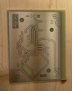
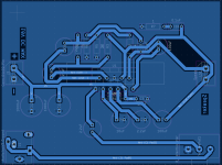
Thank you for all the suggestions and hints on this. I will check them over for sure. I just wanted to post some pictures of the PCB that i etched for it.
It is using a ground plane design for several reasons, mainly its easier on the etch bath.
Now when producing this board in only had a single sided one on hand, so I did need to do some hoops to get everything in as I really did not want to use jumpers, and also I had to design around some physical constraints, mounting holes and heat sink and so on.
Also, to further note, when you say "moving up & down" are you referring to amplitude of the sine-wave? I dont think that is the thing. I will see if i can catch that measurment better. However, I think the FFT distortion measurement is probably the best visible to this. and on that we are just below 1%, maybe 0,7-0,8%
Please have a look at these pictures and see what you think. Some of the ground plane might be a little constrained, however, i calculated them with the thickness and width of the copper to be sure that im within specs.
Have a look and see what you think!
Attachments
Hi!
You PCB looks good, but never tested before. When you follow the PCB suggested by the manufacturer, it has been tested and maybe was a product of other tries they did. In addition, they have a deeper knowleadge and experience with PCB.
I'm not a PCB expert, I just know, by experience, that it is difficult to resolve these oscillations due to PCB adding capacitances, inductances and resistances that are not reflected to the schematics, thus, not considered by the circuit designer.
What you can do is to play around with small capacitors to see if you are able to kill the oscillations.
Examples I would try (not something scientifically calculated, just trials and errors):
-Right in the +V input, you have 2 electrolitycs - you can add the 100nF film capacitor (or more) in parallel - Eletrolitycs are not a short in very high frequencies.
-Along the +V track, you can add the 100nF to GND (it seams C3 already does that, if yes you can increase this value or connect the to another GND point)
-You have 2 RC on amp output (R6/C9 and R7/C10), you can increase the capacitance, but adding a 100nF in parallel. In can also add another RC in another PCB point - remember, a PCB track from capacitor up to the IC lead may be adding an inductance, so if you change the point, you change that inductance.
-You can also try to add a similar RC (100nF/1ohm) directly from one amp to the another amp (in parallel with speaker) - you can vary the resistor too.
-You can try a lower gain, by increasing the R4 and R5 (e.g from 12ohms to 47ohms) - The idea here is that an amp oscillates under certain conditions of gain and phase rotation on feedback. By changing the gain, maybe you put the amplifier in another condition where it doesn't oscillate.
-Following the same previous idea, you can add some small capacitances (1nF, 10nF etc) in parallel with the feedback resistors (R2/R3) to try to move the amp away from the oscillation conditions.
Yes, as the sinewave moves up and down, the amp is placed in different conditions of voltage and current.
In some combinations of V and I it might oscillate, you will see as the sinewave moves up and down that the oscillations only occur at a certain region.
That was the case when I first built the circuit in the protoboard. See below.
These oscillations, in general, occurs in very high frequencies (100kHz, 200kHz etc) and gets superimposed to the audio signal (e.g. 1kHz) causing the distortion you see in frequency domain.

So, you need to observe the sinewave on different amplitudes, load and frequency conditions and check if there is any oscillation.
If yes, then try the suggestions I gave above to try to eliminate these oscillations.
Also inject a 1kHz square wave to observe how your amp behaves.
These time domain observations is a must when you build an audio amp.
Take a print of your sinewave in time domain with the amp loaded when you see the distortion in frequency domain.
You PCB looks good, but never tested before. When you follow the PCB suggested by the manufacturer, it has been tested and maybe was a product of other tries they did. In addition, they have a deeper knowleadge and experience with PCB.
I'm not a PCB expert, I just know, by experience, that it is difficult to resolve these oscillations due to PCB adding capacitances, inductances and resistances that are not reflected to the schematics, thus, not considered by the circuit designer.
What you can do is to play around with small capacitors to see if you are able to kill the oscillations.
Examples I would try (not something scientifically calculated, just trials and errors):
-Right in the +V input, you have 2 electrolitycs - you can add the 100nF film capacitor (or more) in parallel - Eletrolitycs are not a short in very high frequencies.
-Along the +V track, you can add the 100nF to GND (it seams C3 already does that, if yes you can increase this value or connect the to another GND point)
-You have 2 RC on amp output (R6/C9 and R7/C10), you can increase the capacitance, but adding a 100nF in parallel. In can also add another RC in another PCB point - remember, a PCB track from capacitor up to the IC lead may be adding an inductance, so if you change the point, you change that inductance.
-You can also try to add a similar RC (100nF/1ohm) directly from one amp to the another amp (in parallel with speaker) - you can vary the resistor too.
-You can try a lower gain, by increasing the R4 and R5 (e.g from 12ohms to 47ohms) - The idea here is that an amp oscillates under certain conditions of gain and phase rotation on feedback. By changing the gain, maybe you put the amplifier in another condition where it doesn't oscillate.
-Following the same previous idea, you can add some small capacitances (1nF, 10nF etc) in parallel with the feedback resistors (R2/R3) to try to move the amp away from the oscillation conditions.
Also, to further note, when you say "moving up & down" are you referring to amplitude of the sine-wave? I dont think that is the thing. I will see if i can catch that measurment better. However, I think the FFT distortion measurement is probably the best visible to this. and on that we are just below 1%, maybe 0,7-0,8%
Yes, as the sinewave moves up and down, the amp is placed in different conditions of voltage and current.
In some combinations of V and I it might oscillate, you will see as the sinewave moves up and down that the oscillations only occur at a certain region.
That was the case when I first built the circuit in the protoboard. See below.
These oscillations, in general, occurs in very high frequencies (100kHz, 200kHz etc) and gets superimposed to the audio signal (e.g. 1kHz) causing the distortion you see in frequency domain.
So, you need to observe the sinewave on different amplitudes, load and frequency conditions and check if there is any oscillation.
If yes, then try the suggestions I gave above to try to eliminate these oscillations.
Also inject a 1kHz square wave to observe how your amp behaves.
These time domain observations is a must when you build an audio amp.
Take a print of your sinewave in time domain with the amp loaded when you see the distortion in frequency domain.
Hello,
Thanks for checking the PCB out, glad to hear that it was not something super majorly wrong with it at first glance at least!
I would like to note that I did already lower the gain with 56ohm instead of 12ohm. This was done when i moved from a protoboard to this pcb, as i thought it was way to sensitive to noisy input. (Tested it with a PC that i have on the bench, which has incredibly bad output). But by lowering the gain, i got it to behave like my JBL speaker, the bad noise still there, but way way way way better. So that made me happy with the lower gain and went ahead with that.
Before testing the ideas with all the caps and changes, I did take new measurements. And as noticed earlier, I do not really pickup these thick bands of oscillations as you do in your screenshot.
What happens is only that the amplitude is lowered a bit with load compared to without, and of course the noise at 2khz is shown on the FFT screen.
Please see my attached images of the measurement, they come in pair, one FFT and one scope view, without touching anything besides removing the load.
This time I did play file without added distortion, just so that does not play any tricks on us.
With 4ohm load:


Without load:


The bandwidth of the scope is 25mhz, I think this should be enough to catch the issue? My bench-scope has much higher bandwidth, but its a little more troublesome to share screenshots from. However, the waveform does not show the thick oscillation peaks on that one either, so I don't think there is a measuring issue there.
Have a look on these measurements and let me know what you think. I will keep the design static until checked, just to not mess with it further until then.
Thanks!
Thanks for checking the PCB out, glad to hear that it was not something super majorly wrong with it at first glance at least!
I would like to note that I did already lower the gain with 56ohm instead of 12ohm. This was done when i moved from a protoboard to this pcb, as i thought it was way to sensitive to noisy input. (Tested it with a PC that i have on the bench, which has incredibly bad output). But by lowering the gain, i got it to behave like my JBL speaker, the bad noise still there, but way way way way better. So that made me happy with the lower gain and went ahead with that.
Before testing the ideas with all the caps and changes, I did take new measurements. And as noticed earlier, I do not really pickup these thick bands of oscillations as you do in your screenshot.
What happens is only that the amplitude is lowered a bit with load compared to without, and of course the noise at 2khz is shown on the FFT screen.
Please see my attached images of the measurement, they come in pair, one FFT and one scope view, without touching anything besides removing the load.
This time I did play file without added distortion, just so that does not play any tricks on us.
With 4ohm load:
Without load:
The bandwidth of the scope is 25mhz, I think this should be enough to catch the issue? My bench-scope has much higher bandwidth, but its a little more troublesome to share screenshots from. However, the waveform does not show the thick oscillation peaks on that one either, so I don't think there is a measuring issue there.
Have a look on these measurements and let me know what you think. I will keep the design static until checked, just to not mess with it further until then.
Thanks!
Hi!
Your sinewave in time domain looks clean - I cannot see any oscillation.
As long as you see this clean shape in all conditions of output power, load and frequency, I don't see any major issue.
I mentioned frequency, cause in a reactive load such as a speaker, impedance is variable so the amp must be stable in all frequencies.
One thing you can try is to put an external short thick wire (just carefully touching the two ends) to bypass the thin tracks that carry high current to see if there is any difference in 2nd harmonic distortion. This are the tracks that connect IC output pins to speaker. GND track has a lot of area since you opt for a GND plane, so I don't see problems here.
The frequency domain is better viewed using dB scale in order to accomodate high (fundamental) and low (harmonics) numbers and you can effective measure the distortion. Try this setup so you can measure the THD.
- Home
- Amplifiers
- Chip Amps
- TDA2004 Bridge configuration, distortion/2nd harmonic?