Why did this one use Inverter on Data and Fsynk?
An externally hosted image should be here but it was not working when we last tested it.
The difference would be, in his Retro- Dac he uses one AD1865 for L +/- and one for R +/-, whereas this would use one chip for L/R + and one for L/R -. What are advantages/disadvantages?
An externally hosted image should be here but it was not working when we last tested it.
till said:The difference would be, in his Retro- Dac he uses one AD1865 for L +/- and one for R +/-, whereas this would use one chip for L/R + and one for L/R -. What are advantages/disadvantages?
The picture you posted hasn't a DAC for L+- and one for R+-
Each dac has L AND R, one has the + the second has the -
whereas this would use one chip for L/R + and one for L/R -
Thats what i said.
the thread will not be more easy to read by quoting pictures
ok, I've read to fast.
but inverting the dataline (-> havine one dac for r+ l+ and one for r- l-) is a far more easy solution. At least for I2S signals.
but inverting the dataline (-> havine one dac for r+ l+ and one for r- l-) is a far more easy solution. At least for I2S signals.
Using Xor gates is better than the inverter
I don't precisely know the audible effect of time differences between the non-inverted and inverted signals, but they can be simply preventd by using xor-logic for both signals.
Connect L and R to each input of a separate XOR-gate (74ls86)and connect the other input to 0 (you get L+ and R+). Mirror this solution but connect inputs to 1 and you get L- and R-.
I wonder if there is a better solution to this (in terms of jitter) and not considering asynchronous reclocking. Should the CLK also be considere.
So the point is phase difference between the Data and INV(Data) is not exactly 180° with inverter in one line? are there high speed inverterts?
Or what about a unity gain phase splitter (one transistor) or a differential pair instead of inverter?
Or what about a unity gain phase splitter (one transistor) or a differential pair instead of inverter?
You can probably split the datastream with anything. In the general scheme of things I doubt that it adds up to much, though I am sure there are those who are certain to claim they can discern a difference between a circuit with the inverter and one with the xor while at the same time overlooking the lack of LSB inversion.
The idea behind using one dac for L and L- is that any noise generated in the dac common to both channels is rejected when the outputs are summed.
ray
The idea behind using one dac for L and L- is that any noise generated in the dac common to both channels is rejected when the outputs are summed.
ray
OK, this reason i do understand.
Would this work?
Any idea were i could obtain the connector for I2S out on my CD PRO2?
Would this work?
An externally hosted image should be here but it was not working when we last tested it.
Any idea were i could obtain the connector for I2S out on my CD PRO2?
or this
Still don´t know how to set mode at OB/TWC and how to obtain the damned I2S connector of CD PRO2
An externally hosted image should be here but it was not working when we last tested it.
Still don´t know how to set mode at OB/TWC and how to obtain the damned I2S connector of CD PRO2
OD should go to pen 28, as for normal i2s.
http://www.diyaudio.com/forums/showthread.php?threadid=8614&perpage=15&highlight=&pagenumber=2
As Ray pointed out: inverting the dataline is not a 100% inversion of the signal. The correct procedure would be : invert bit 2 to 16, but do not invert bit 1 (LSB). So by inverting the dataline, you're one bit off.
You have connected the i2s signals incorrect to the tda
In one of your previous posts you connected 180 i/v resistor to the tda1541. That is way too high, i'll get distortion. Check some posts/designs.
Put i see new idea's for i/v ciruits 😀 😀
Greetings,
guido said:OD should go to pen 28, as for normal i2s.
http://www.diyaudio.com/forums/showthread.php?threadid=8614&perpage=15&highlight=&pagenumber=2
As Ray pointed out: inverting the dataline is not a 100% inversion of the signal. The correct procedure would be : invert bit 2 to 16, but do not invert bit 1 (LSB). So by inverting the dataline, you're one bit off.
You have connected the i2s signals incorrect to the tda
In one of your previous posts you connected 180 i/v resistor to the tda1541. That is way too high, i'll get distortion. Check some posts/designs.
Put i see new idea's for i/v ciruits 😀 😀
Greetings,
Oeps, OB i mean
Put i see new idea's for i/v ciruits
sorry, its not new, its Pass... as seen on www.passlabs.com
thanks for corrections.
Thought so, but as far as i remember the pass design used the PCM63 with the current source connected.
Therefore signal in with zero's (mute, no signal) would output
0 mA to the output circuits.
The TDA is -2mA at zero's in and has no current cource to corrrect.
Look at pedja's AD844 design were he uses a current source to correct this.
Guido
Therefore signal in with zero's (mute, no signal) would output
0 mA to the output circuits.
The TDA is -2mA at zero's in and has no current cource to corrrect.
Look at pedja's AD844 design were he uses a current source to correct this.
Guido
Till,
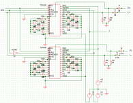
The second circuit should work giving +(L/R) and -(L/R) and datasheet covers OB/TWC. BTW, OB is for simultaneous mode only.
The first circuit will not work as the data is I2S. Multibit AD dacs are LSB justified. I2S is MSB justified to 1 serial clock cycle after a L/R clock transition. If the format was correct, there would be an interchannel delay of 11microseconds.
IHO, the easiest way to get +-R and +-L would be to convert the I2S to another format, that uses different lines for L and R
Then, simply feed the DAC with digital L (or R) at one input, and inverted digital L (or R) at the other input
Then, simply feed the DAC with digital L (or R) at one input, and inverted digital L (or R) at the other input
second circuit is posting #32 and first circuit posting #31, right?
so at the #32 circuit i have to look at this -2mA / current source problem.
How do i connect an AD DAC to I2S? or is it only possible with SPDIF and reciver chip?
And an answer for the connector problem?
What is wrong and how is it right? what # ?
good idea - with any chip, or with a microcontroler / DSP? how fast do i need to feed the DAC / what is the I2S clock? 2,82MHz like in DDDAC?
so at the #32 circuit i have to look at this -2mA / current source problem.
How do i connect an AD DAC to I2S? or is it only possible with SPDIF and reciver chip?
And an answer for the connector problem?
You have connected the i2s signals incorrect to the tda
What is wrong and how is it right? what # ?
the easiest way to get +-R and +-L would be to convert the I2S to another format, that uses different lines for L and R
good idea - with any chip, or with a microcontroler / DSP? how fast do i need to feed the DAC / what is the I2S clock? 2,82MHz like in DDDAC?
- I have seens loads of circuit connecting some DAC with recivers (8412 or 8414) to SPDIF, but not to I2S.
Is this better or still wrong? #40
- I don´t understand / find this current source issue in D1 circuit, some hint?
- What abaut TDA1543, same problem when I/V with D1 stage?
Is this better or still wrong? #40
An externally hosted image should be here but it was not working when we last tested it.
- I don´t understand / find this current source issue in D1 circuit, some hint?
- What abaut TDA1543, same problem when I/V with D1 stage?
- Status
- Not open for further replies.
- Home
- Source & Line
- Digital Source
- TDA1541A/S1 Arrangements