First try to separate left and right for +/- per each chip.
No conversion to ninary offset yet.
Still only simple data inversion.
What ya think ?
1541 is in simultaneous data mode.

No conversion to ninary offset yet.
Still only simple data inversion.
What ya think ?
1541 is in simultaneous data mode.
what mode is this?? how does the TDA1541 know to use separate lines and split the channels? they told me one data (R) line needs in the normal I2S mode the bitclock.
Rah has already done the bulk of the work required to create a balanced dac using the TDA1541/A in simultaneous mode. His circuit requires some modification as it assumes serial clock is 32Fs. Further modification will also be required to invert the LSB (equivalent to adding 1).
ray.
ray.
Till,
it is simultaneous data mode, so called in the datasheet..
One latch enable signal = FSYNC.
Two data channels left and right.
One clock signal.
If Fsync goes L, after one SCK the data of both channels of the chip (!) will be loaded.
If it goes high, the data will be stored.
So what we need is a counter for each chip, which after Fsync transition inverts the data line until two clock cycles and then resets.
This we need for conversion to offset binary.
The 1541 datasheet is so bad that the best will be trial and error....
ray,
any link to a schematic ?
it is simultaneous data mode, so called in the datasheet..
One latch enable signal = FSYNC.
Two data channels left and right.
One clock signal.
If Fsync goes L, after one SCK the data of both channels of the chip (!) will be loaded.
If it goes high, the data will be stored.
So what we need is a counter for each chip, which after Fsync transition inverts the data line until two clock cycles and then resets.
This we need for conversion to offset binary.
The 1541 datasheet is so bad
that the best will be trial and error....ray,
any link to a schematic ?
rah posted schematics in this thread http://www.diyaudio.com/forums/showthread.php?s=&threadid=25608
but i don´t understand, too much logic...
Philips seems to write much less informative datasheets than Texas Instruments f.e.
but i don´t understand, too much logic...
Philips seems to write much less informative datasheets than Texas Instruments f.e.
I have a Technics LS-P770 that uses 4 x PCM56.
Is this balanced ?
Now I got the I2SBUS.PDF and for sure we will get this working.
And then I will maybe built the balanced 2x4chip parallel monster DAC
Is this balanced ?
Now I got the I2SBUS.PDF and for sure we will get this working.
And then I will maybe built the balanced 2x4chip parallel monster DAC
little off topic
I have some incredible push buttons with built in lcd graphic display, bi-color background lighting.
This has very few wires, not more than 4 I guess.
Could that be I2S ? Or what other interface ?
I have some incredible push buttons with built in lcd graphic display, bi-color background lighting.
This has very few wires, not more than 4 I guess.
Could that be I2S ? Or what other interface ?
Since there are not that many people happy with GAL's i tried to
do without. So i took some stuff out of the GAL design (mute, choice of differential) and put all in normal logic.
This is just a quick drawing, could be with mistakes (check the clock)
In: I2S, out I2S +R/-R and I2S +L/-L
With:
1 HEF4517 philips
2 74F64
1 '175 FF
1 '74 FF
1 '04 INV
Dont look at the logic types, just used what i found first in the library. And i did not cleanup at all.
This thing should work, but if you are really going ahead here compare the (working) GAL based design with this to make shure.
AND CHECK FIRST IF YOU CAN GET THE 74x64
It a Four-Two-Three-Two-Input AND.OR.Invert gate
A GAL would replace those '64s and the INV. Chipcount: 4 😀
Just to give you some idea's 😀 😀 😀
Greetings,
Attachments
better a GAL + 3chips than no gal and 7 chips!
I have nothing against the GAL, i only don´t have a GAL programmer. Sould try to build one.
- rfbrw postet
- again: i don´t see how inverting LSB is = adding one, as the 2nd LSB isn´t incremented in case LSB goes to zero.
Better don´t do anything with LSB and live with offset, or do a real twos complement inversion with a processor.
- The logic for splitting I2S in L/R: couldn´t the logic also, provide me with a WCLK with 19BCKL time offset to normal WCKL? so it would be also left justifief for AD chip...
- And any idea for the I2S connectors JSP 2mm for CD PRO2 ? were to buy?
- The 74F64 and HEF4517 not at Reichelt, MOS4517 yes
I have nothing against the GAL, i only don´t have a GAL programmer. Sould try to build one.
- rfbrw postet
Further modification will also be required to invert the LSB (equivalent to adding 1).
- again: i don´t see how inverting LSB is = adding one, as the 2nd LSB isn´t incremented in case LSB goes to zero.
Better don´t do anything with LSB and live with offset, or do a real twos complement inversion with a processor.
- The logic for splitting I2S in L/R: couldn´t the logic also, provide me with a WCLK with 19BCKL time offset to normal WCKL? so it would be also left justifief for AD chip...
- And any idea for the I2S connectors JSP 2mm for CD PRO2 ? were to buy?
- The 74F64 and HEF4517 not at Reichelt, MOS4517 yes
Re inverting the LSB.
It is indeed correct that simply inverting the LSB is a bit of a hit-and-miss affair and as such my description of the added logic and what it does was incorrect. The circuitry in question is actually a bit-serial adder.
It is indeed correct that simply inverting the LSB is a bit of a hit-and-miss affair and as such my description of the added logic and what it does was incorrect. The circuitry in question is actually a bit-serial adder.
Err,Guido, it does not work. For a start the 4-input and-gate is clocked with WS and WS inverted which in practice means its output is always low. There is also WS delayed by a flip-flop clocked with inverted serial clock which causes a runt pulse in the data. But that can all be remedied.
What cannot be so easily dealt with from the CDPro2 point of view is that the circuit assumes serial clock is 64Fs. The CD Pro2 outputs a serial clock of 48Fs.
ray.
What cannot be so easily dealt with from the CDPro2 point of view is that the circuit assumes serial clock is 64Fs. The CD Pro2 outputs a serial clock of 48Fs.
ray.
ray, you advice is invaluable as you are the only one here who seems to really know all about the DACs and dataformats.
Bernhard wants to connect the DACs (TDA1541) balanced and simlutanous ( as we have a phase offset else) to a reciver chip / CS8412. I would prefer to use CD PRO2 I2S output without reciver, as i expect much more clock error using SPDIF than I2S.
We look for a solution that ideally fits all needs. Else i have to use a CS8412 also - and need advice on how usefull and necessary what kind of reclocking would be.
Also i would like to connect the AD chip to compare different ones.
Until now i´m lucky i got the minimal version with TDA1543 and inverter to work in an acceptable way.
Wow, this thread has grown huge!
I don’t know what happened to my subscription, I wasn’t even aware of all the things going on in here. 🙂
Anyway guys, like I promised before, that circuit I was previously working on is here. You know all about it from Ray’s (rfbrw) and my conversation on: http://www.diyaudio.com/forums/showthread.php?s=&threadid=25608
Today, after having a quick wiz through this thread, I thought I might take out some time and at least put something up. So here it is, I was working on it before, and have put in a document today. It’s a rushed job, bound to have mistakes! 🙂 But, hopefully you’ll find it useful. It has been simulated, graphs attached, but I have not tested it.
Keep up the good work on diyAudio!
Rahul.
Attachments
Some more reactions:
Till: the GAL could actually replace '64, '04 and the '175. 3 Chips remaining... I did nothing with the LSB 'issue' here.
WS is delayed with 1 BCK. To delay it more you could: use 4517 to delay it with 16 and two more '74 to delay it 1+16+2=19 BCK. But probably some form of counter on BCK is better.
btw, GAL's are small, they can be delivered by post...
I2S connector: no.
74F64 will be a problem. 4517 must be able to handle the clockspeed. Check the datasheet. Philips is 5MHz typical, so ok.
Bernhard, this is for I2S, so time multiplexed. So it should also work for TDA1543 etc.
Ray, 4-AND should be C,D,E,F which is /WS,data32,WSdelay,vcc.
This should be done with the 74F64's, the use of the second half of the 4517, the inverters and the '175 (a copy from the GAL content):
DATAR :=
WS * DATA +
/WS * SHIFT32 * WSDELAY +
/WS * /SHIFT32 * /WSDELAY
DATAL :=
WS * SHIFT32 +
/WS * SHIFT64 * WSDELAY +
/WS * /SHIFT64 * /WSDELAY
:= in GAL terms is registered output, clock low to high.
should be:
A * B +
C * D * E +
G * H * I
F = High, unsed and J,K = low, unused. But it was a rush job, so there could be mistakes in there.
Since the output is a NOR, i used the inverted outputs of the '175.
Remember, i just took the GAL content and put it into logic. The GAL version works, so this should work too....
The WS delayed is created by the two ff's both delaying ws by half a BCK.
One other thing is timing, i did not check if the '175 ff does the job as the GAL:
Quote from 2 TDA1541 post: "The clock from pin 21 is also used to latch the registered outputs of the GAL via pin1.... Registered outputs can be made registered by using ":=" in the declaration. This is used for data and ws (later). So the shift register and the GAL are both clocking on low to high. Strange? Well suppose the MSB just came out of the fifo, therefore it is available at pin6 of the GAL. It is also available at pin 9 of U6, the shift register.
Before clocking, the previous MSB will be in cell 32 of the register and available at pin10 of U6 and the MSB before at pin11. When clock goes low to high the GAL will therefore clock the MSB's: all is in sync. The logic clocks on the same clock, but some (in case of the 4517, many) nanoseconds later the data will be at the output pins. But then the correct bit is already clocked by the GAL.. Hihi. According to the databook, the holdtime after clock goes low to high is 0 nanosec minimum for the GAL. That's why this is possible."
====
This was just to show that it is possible to build a I2S splitter with logic.
Rahul, Ray,
Any idea if the parallel mode is better in terms of jitter towards the TDA1541. Just wondering??
Regards,
guido, so it looks like i have to build a GAL programmer
with those I2S connector i will have a real problem. Maybe i need to buy a second CD PRO and tell Nico to send it with 10+ of those connectors.
The advantage of time multiplexed mode with 1541 i see is the SCK line for a precision clock for the DAC. This is lost with in the other mode.
But does the DAC output the sample for left and right channel at the same moment in time multiplexed mode? and if feed in simultaneously mode, but first one channel, than the other, (what i interpret rahs diagramms) , will the samples of left and right channel appear at the same moment at the output?
edit:
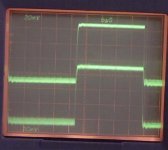
i measured time multiplexed mode with TDA1543 20kHz from test CD the samples left/right are absolutely in phase. (i wish i had a few really good scope probes)
with those I2S connector i will have a real problem. Maybe i need to buy a second CD PRO and tell Nico to send it with 10+ of those connectors.
The advantage of time multiplexed mode with 1541 i see is the SCK line for a precision clock for the DAC. This is lost with in the other mode.
But does the DAC output the sample for left and right channel at the same moment in time multiplexed mode? and if feed in simultaneously mode, but first one channel, than the other, (what i interpret rahs diagramms) , will the samples of left and right channel appear at the same moment at the output?
edit:
i measured time multiplexed mode with TDA1543 20kHz from test CD the samples left/right are absolutely in phase. (i wish i had a few really good scope probes)
Attachments
till said:guido, so it looks like i have to build a GAL programmer
The advantage of time multiplexed mode with 1541 i see is the SCK line for a precision clock for the DAC. This is lost with in the other mode.
But does the DAC output the sample for left and right channel at the same moment in time multiplexed mode? and if feed in simultaneously mode, but first one channel, than the other, (what i interpret rahs diagramms) , will the samples of left and right channel appear at the same moment at the output?
Do R+/L+ R-/L- or build a GAL programmer or use one of the schematics without a GAL or ask somebody who has a programmer to sent you a programmed GAL..
 😉 😀
😉 😀 Plenty of options.
i think the DAC outputs left and right at the same moment for all modes. That will be in the datasheet. For I2S it should do this based on WS and for the parallel mode on LE (not shure, check the datasheet) 😱
Greetings,
First i will work on the I/V stage (D1 like) and start with simpel inverter. Time offset of 6ns is not much. Later i will ask you for a GAL. And i hope we find a solution for AD chips also. I hace 1865 and 1861 and i want to test them.
till said:The advantage of time multiplexed mode with 1541 i see is the SCK line for a precision clock for the DAC. This is lost with in the other mode.
Who says that it is lost ? It is still there.
I would be happy if the schematic posted by Rahul works.
I have made progress with my own also.
Will post it soon, is maybe more simple.
- Status
- Not open for further replies.
- Home
- Source & Line
- Digital Source
- TDA1541A/S1 Arrangements